JAJSD34C April 2017 – April 2018 CSD88599Q5DC
PRODUCTION DATA.
- 1特長
- 2アプリケーション
- 3概要
- 4改訂履歴
- 5Specifications
-
6Application and Implementation
- 6.1 Application Information
- 6.2 Brushless DC Motor With Trapezoidal Control
- 6.3 Power Loss Curves
- 6.4 Safe Operating Area (SOA) Curve
- 6.5 Normalized Power Loss Curves
- 6.6 Design Example – Regulate Current to Maintain Safe Operation
- 6.7 Design Example – Regulate Board and Case Temperature to Maintain Safe Operation
- 7Layout
- 8デバイスおよびドキュメントのサポート
- 9メカニカル、パッケージ、および注文情報
パッケージ・オプション
デバイスごとのパッケージ図は、PDF版データシートをご参照ください。
メカニカル・データ(パッケージ|ピン)
- DMM|22
サーマルパッド・メカニカル・データ
発注情報
6.7.3 Calculating SOA Adjustments
- SOA adjustment for switching frequency ≈ 1.3°C (Figure 4)
- SOA adjustment for input voltage ≈ 0.1°C (Figure 5)
- SOA adjustment for duty cycle ≈ 0.7°C (Figure 6)
- Final calculated SOA adjustment = 1.3 + 0.1 + 0.7 ≈ 2.1°C
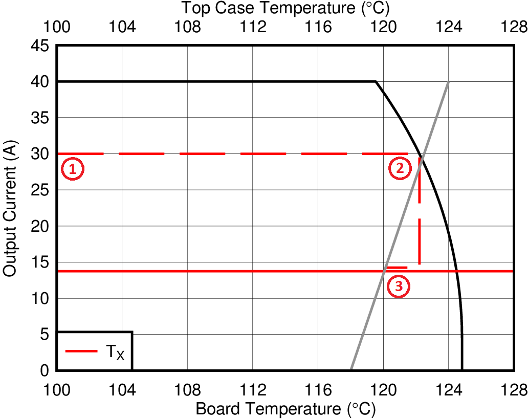
In the Design Example – Regulate Current to Maintain Safe Operation section above, the estimated power loss of the CSD88599Q5DC would increase to 4.7 W. In addition, the maximum allowable board temperature would have to increase by 2.1°C. In Figure 21, the SOA graph was adjusted accordingly.
- Start by drawing a horizontal line from the application current (30 A) to the SOA curve.
- Draw a vertical line from the SOA curve intercept down to the TX line.
- Adjust the intersection point by subtracting the temperature adjustment value.
In this design example, the SOA board/ambient temperature adjustment yields a decrease of allowed junction temperature of 2.1°C from 122.2°C to 120.1°C. Now it is known that the intersection of the case and PCB temperatures on the TX line must stay below this point. For instance, if the power block case is observed operating at 124°C, the PCB temperature must in turn be kept under 118°C to maintain this crossover point.
