SNOSCS3B September 2013 – March 2014 LMP91300
PRODUCTION DATA.
- 1 Features
- 2 Applications
- 3 Description
- 4 Revision History
- 5 Terminal Configuration and Functions
- 6 Specifications
-
7 Detailed Description
- 7.1 Overview
- 7.2 Functional Block Diagram
- 7.3 Feature Description
- 7.4 Device Functional Modes
- 7.5 Programming
- 7.6
Register Maps
- 7.6.1 DET_H_MSB_INIT - Detection High Threshold MSB (Initial) (Address 0x66)
- 7.6.2 DET_H_LSB_INIT - Detection High Threshold LSB (Initial) (Address 0x67)
- 7.6.3 DET_L_MSB_INIT - Detection Low Threshold MSB (Initial) (Address 0x68)
- 7.6.4 DET_L_LSB_INIT - Detection Low Threshold LSB (Initial) (Address 0x69)
- 7.6.5 INFO0 - Device Information 0 (Address 0x6A)
- 7.6.6 INFO1 - Device Information 1 (Address 0x6B)
- 7.6.7 INFO2 - Device Information 2 (Address 0x6C)
- 7.6.8 INFO3 - Device Information 3 (Address 0x6D)
- 7.6.9 OSC_CONFIG_0 - Oscillator Configuration 0 Register (Address 0x6E)
- 7.6.10 45
- 7.6.11 OSC_CONFIG_1 - Oscillator Configuration 1 Register (Address 0x6F)
- 7.6.12 OSC_CONFIG_2 - Oscillator Configuration 2 Register (Address 0x70)
- 7.6.13 OSC_CONFIG_3_INIT - Oscillator Configuration 3 Register (Initial) (Address 0x71)
- 7.6.14 OUT_CONFIG_INIT - Output Configuration Register (Initial) (Address 0x72)
- 7.6.15 DET_H_MSB_FNL - Detection High Threshold MSB (Final) (Address 0x73)
- 7.6.16 DET_H_LSB_FNL - Detection High Threshold LSB (Final) (Address 0x74)
- 7.6.17 DET_L_MSB_FNL - Detection Low Threshold MSB (Final) (Address 0x75)
- 7.6.18 DET_L_LSB_FNL - Detection Low Threshold LSB (Final) (Address 0x76)
- 7.6.19 OSC_CONFIG_3_FNL - Oscillator Configuration 3 Register (Final) (Address 0x77)
- 7.6.20 OUT_CONFIG_FNL - Output Configuration Register (Final) (Address 0x78)
- 7.6.21 TEMP64 - Temperature In °C + 64 (Address 0x79)
- 7.6.22 PROXIMITY_MSB - Proximity MSB (Address 0x7A)
- 7.6.23 PROXIMITY_LSB - Proximity LSB (Address 0x7B)
- 7.6.24 STATUS - Device Status (Address 0x7E)
- 7.6.25 BURN_REQ - Burn Request (Address 0x7F)
-
8 Application and Implementation
- 8.1 Application Information
- 8.2
Typical Application
- 8.2.1 Design Requirements
- 8.2.2
Detailed Design Procedure
- 8.2.2.1 Quick Start
- 8.2.2.2 Determining The RP of an LC Tank
- 8.2.2.3 Component Selection And Layout
- 8.2.2.4 CF (CFA and CFB Terminals)
- 8.2.2.5 NTC (TEMP+ Terminal)
- 8.2.2.6 C1
- 8.2.2.7 CV+/EXT E
- 8.2.2.8 CBY (CBY Terminal)
- 8.2.2.9 RSENSE
- 8.2.2.10 REXT B (EXT B Terminal):
- 8.2.2.11 R1
- 8.2.2.12 SENSE1+ And SENSE2+ Terminals (RSENSE1+, RSENSE2+)
- 8.2.2.13 NPN
- 8.2.2.14 PNP
- 8.2.2.15 LED
- 8.2.2.16 LC Tank and INA and INB Terminals
- 8.2.2.17 SWDRV Terminal
- 8.2.2.18 P1 To P5 Terminals
- 8.2.2.19 GND Terminals
- 8.2.2.20 NC Terminals
- 8.2.2.21 Exposed DAP
- 8.2.2.22 SENSE-
- 8.2.3 Look-Up Table Calibration
- 9 Power Supply Recommendations
- 10Layout
- 11Device and Documentation Support
- 12Mechanical, Packaging, and Orderable Information
パッケージ・オプション
メカニカル・データ(パッケージ|ピン)
サーマルパッド・メカニカル・データ
発注情報
8 Application and Implementation
8.1 Application Information
The LMP91300 is a complete analog front end (AFE) optimized for use in inductive proximity sensors. The LMP91300 detects the presence of a metal object based on the RP change of an LC oscillator, depending on the distance of the metal object.
The LMP91300 can be used in 3 wire NPN or PNP inductive sensors.
8.2 Typical Application
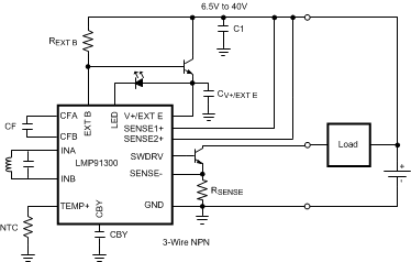 Figure 19. 3-Wire NPN Configuration
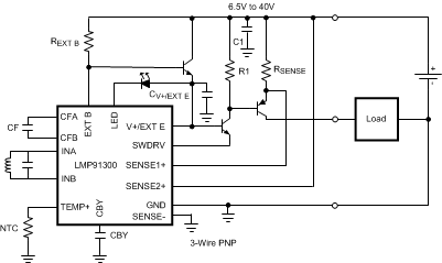 Figure 20. 3-Wire PNP Configuration
For operation above 40V a series resistance must be added to SENSE1+ and SENSE2+. The mismatch in these resistors will affect the overload protection accuracy for the PNP configuration. These resistors must be chosen so that the SENSE1+ and SENSE2+ terminals do not operate above 40V.
8.2.1 Design Requirements
- Loop Voltage: 6.5V to 40V
- LC Tank Oscillation Frequency: 0.005MHz to 5MHz
- LC Tank RP: 798Ω to 3.93MΩ
8.2.2 Detailed Design Procedure
8.2.2.1 Quick Start
When a new sensor is being used the registers should be setup using the following procedure. Instructions on how to determine the value to put in each register are described in the Register Maps section.
- Set RP_MAX in the OSC_CONFIG_0 register.
- Set PADC_TIMEC and RP_MIN in the OSC_CONFIG_1 register.
- Set RESONATOR_MIN_FREQ in the OSC_CONFIG_2 register.
- Set UNDER_RANGE_SWITCH_EN, OSC_AMP, and RESPONSE_TIME in the OSC_CONFIG_3_INIT and OSC_CONFIG_3_FNL registers. The same values should be written to both registers. Setting OSC_AMP to 4V and RESPONSE_TIME to 6144 should give the most accurate results. Note that the power on default for OSC_AMP is 11:Reserved so OSC_AMP must be changed to either 1V, 2V, or 4V.
- Select the value of the CF capacitor as described in the CF (CFA and CFB Terminals) section.
- Set the values in the OUT_CONFIG_INIT and OUT_CONFIG_FNL registers as needed. The same values should be written to both registers.
- Put the sensor at the target distance that the switch is supposed to turn on. Read the PROXIMITY_MSB and Proximity LSB multiple times. If needed, RP_MAX or RP_MIN can be adjusted up or down one step at a time to determine the combination that gives the most accurate setting for this specific sensor.
- Put the sensor at the target distance that the switch is supposed to turn on. Read the PROXIMITY_MSB and Proximity LSB multiple times, take an average, and write this value into the DET_H_MSB_INIT and DET_H_LSB_INIT and DET_H_MSB_FNL and DET_H_LSB_FNL registers. This value may need to be adjusted.
- Put the sensor at the target distance that the switch is supposed to turn off. Read the PROXIMITY_MSB and Proximity LSB multiple times, take an average, and write this value into the DET_L_MSB_INIT and DET_L_LSB_INIT and DET_L_MSB_FNL and DET_L_LSB_FNL registers. This value may need to be adjusted.
8.2.2.2 Determining The RP of an LC Tank
The method in the Quick Start section for setting the values in the LMP91300 registers requires that the RP of the LC tank be known at the switching point (the point that the switch is changed from the normal condition to the triggered condition). It is best to use an impedance analyzer to characterize the RP of the LC tank over distance. If an impedance analyzer is not available the RP of the LC tank can be determined using the method below.
- Set the target at the switching distance from the sensor.
- Set PADC_TIMEC = 1, RESONATOR_MIN_FREQ as described in the Register Maps section, OSC_AMP = 4V, and RESPONSE_TIME = 6144.
- Put a scope probe on INA or INB.
- Step RP_MIN up one step at a time until the amplitude of the signal on the oscilloscope becomes variable as shown in Figure 21 and Figure 22. Increase RP_MIN by two, for example if the amplitude becomes variable at 17, set RP_MIN to 19.
- Step RP_MAX up one step at a time until the amplitude of the signal on the oscilloscope becomes steady. Decrease RP_MAX by two steps, for example if amplitude became steady at 16, set RP_MAX to 14.
- Set the CF capacitor as described in the CF (CFA and CFB Terminals) section.
- Read the Proximity value in registers 0x7A and 0x7B and convert this value to decimal.
- Use the formula RPLCTANK (Ω) = (RP_MAX × RP_MIN ) / ( RP_MIN × (1-Y) + RP_MAX × Y ), where Y = Proximity Data / 2^15 and RP_MAX and RP_MIN are the impedance values shown in Register Maps section.
This value can have a tolerance of ±25% when compared to the value from an impedance analyzer.
8.2.2.3 Component Selection And Layout
The following PCB layout guidelines and suggested components should be used when designing a PCB.
8.2.2.4 CF (CFA and CFB Terminals)
10pF to 100nF, ≥10V, X7R ceramic capacitor. The traces connecting CFA and CFB to the capacitor should be as short as possible to minimize the parasitic capacitance. The value of this capacitor will be based on the time constant and resonating frequency of the LC tank.
For optimal performance, the value of CF, needs to be as small as possible, but large enough such that the active filter does not saturate. The size of this capacitor depends on the time constant of the SENSE coil, which is given by L/RS, (L = inductance, RS = series resistance of the inductor at oscillation frequency). The larger this time constant becomes, the larger the value of filter capacitor that is required. Hence, this time constant reaches its maximum when there is no target present in front of the sensing coil.
The following procedure can be used to determine CF:
- Start with a default value of 10nF for CF.
- Set RP_MAX, PADC_TIMEC, RP_MIN, RESONATOR_MIN_FREQ, OSC_AMP, and RESPONSE_TIME to the desired values as described in the Register Maps section.
- Move the metal target far away from the LC tank.
- Connect a scope probe to the INB (terminal 21) and CFB (terminal 17) terminals. Since the CFB terminal is very sensitive to capacitive loading, it is recommended to use an active probe. As an alternative, a passive probe with a 1kΩ series resistance between the tip and the CFB terminal can be used.
- Set the time scale of the oscilloscope so that many periods of the signal on the INA terminal can be seen. See Figure 21.
- Set the CF capacitor value so that the AC portion of the waveform is about 1VPP maximum. Decreasing the capacitor value will make the AC portion of the waveform larger. This signal scales linearly with the reciprocal of the filter capacitance. For example, if a 100pF filter capacitor is used and the signal observed on the CFB terminal has a peak-to-peak value of 200mV, the desired 1V peak-to-peak value is obtained using a 200mV / 1V × 100pF = 20pF filter capacitor. Figure 21 shows the waveforms on CFB and INA and Figure 22 shows the waveforms using a zoomed in horizontal scale. Note that the waveforms on CFB and INA are not a constant amplitude. The waveform on CFB should be adjusted so that the maximum value is 1VPP.
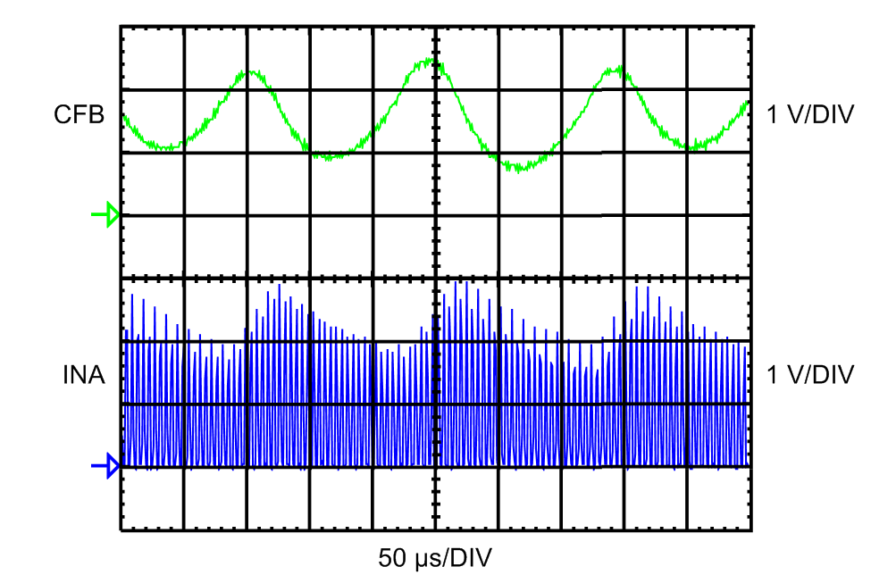 Figure 21. Determining the Value of CF
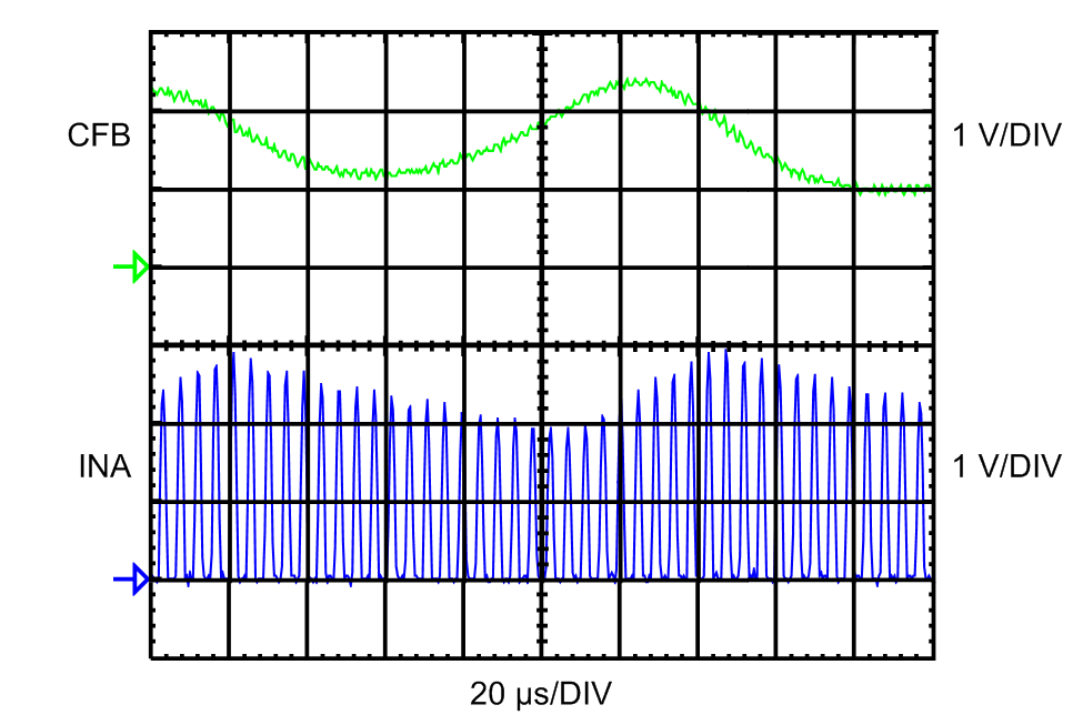 Figure 22. Determining the Value of CF
8.2.2.5 NTC (TEMP+ Terminal)
The thermistor, such as the Murata NCP03WF104F05RL, should be placed as close to the LC tank as possible to minimize error introduced by temperature variation within the operating environment. The NTC should also be close to the LMP91300 to minimize the parasitic capacitance. It is connected between terminals 22 and 23. There should be a ground trace separating the thermistor from the LC tank, to minimize the coupling from the signal on the LC tank. Ideally, the thermistor could be on one side of the PCB and the LC tank on the other side of the PCB with a ground plane between them.
8.2.2.6 C1
0.1µF to 1µF, ≥50V, X7R ceramic capacitor. This is a bypass capacitor for the regulator. The value of this capacitor will also affect the rising and falling edges of the SWIF signal. A good value to start with is 0.1µF.
8.2.2.7 CV+/EXT E
100nF, ≥10V, X7R ceramic capacitor. If the loop voltage is ≤ 8V, 100nF is the maximum value that can be used.
8.2.2.8 CBY (CBY Terminal)
56nF, ≥5V, X7R ceramic capacitor. Connect between the CBY terminal and ground.
8.2.2.9 RSENSE
The value of this resistor and power rating of the RSENSE resistor depends on the amount of current allowed through the switch transistor. The LMP91300 has an Over Current Detection Threshold of 310mV typical. When the LMP91300 detects ≥ 310mV across the sense resistor it will go into Overload Protection mode. In this mode it will periodically turn on the switch for 30µs to check if the overload condition is still there. If the LMP91300 detects a value ≥ 310mV (typical) across the sense resistor it will limit the current through the switch so that the voltage across RSENSE is ≤ 480mV. See the OVERLOAD PROTECTION entries in the ELECTRICAL CHARACTERISTICS section and Figure 7, Figure 12, and Figure 13.
8.2.2.10 REXT B (EXT B Terminal):
The internal regulator along with the external NPN transistor will develop 5V on the V+/EXT E terminal. The EXT B terminal will be one diode drop above this at about 5.6V. The voltage across REXT B will be the difference between the loop voltage and the 5.6V on the EXT B terminal. The value of REXT B depends on the minimum loop voltage and the minimum temperature that the LMP91300 will be used at. The values shown in Figure 23 show the largest typical value for REXT B that can be used for a specific minimum loop voltage and minimum temperature. For example, if the LMP91300 is being used in a proximity sensor that has a specification of 10V minimum for the loop voltage and an operating temperature minimum of 0°C, a value of 26kΩ or smaller can be used for REXT B. The data shown in Figure 23 depends on several variables, such as the external transistor used and the value of CV+/EXT E. A SMBTA06 transistor was used when taking the data in Figure 23. The user must ensure that the resistor has the correct power rating and that the regulated 5V on the V+/EXT E terminal comes up correctly and is stable for the entire loop voltage and temperature range in the intended application.
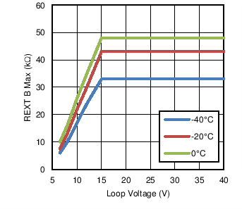 Figure 23. Maximum REXT B Value
8.2.2.11 R1
33kΩ, 1/8W resistor.
8.2.2.12 SENSE1+ And SENSE2+ Terminals (RSENSE1+, RSENSE2+)
If the supply is ≤ 40V these terminals can be shorted to the supply. If the supply is > 40V resistors must be placed between the SENSE1+ and SENSE2+ terminals and the supply. These resistors must drop enough voltage so that the terminals of the LMP91300 are < 40V. The resistors will have 100µA going through them. For example, if the supply is at 50V, 10V will need to be dropped across these resistors so the resistance will be 10V/100µV = 100kΩ. These resistors must be matched resistors, 0.1% or better. Keep the trace between the LMP91300 and the resistors short.
In NPN mode the SENSE1+ terminal is not used. It should be connected to the supply as described above.
8.2.2.13 NPN
A SMBTA06 or similar transistor.
8.2.2.14 PNP
A FMMT593 or similar transistor.
8.2.2.15 LED
The LMP91300 can be programmed to supply 2.5 or 5mA. The LED chosen should have a voltage drop of less than 3V. If an LED is not needed the LED terminal can be connected directly to the V+/EXT E terminal. The LMP91300 uses the LED terminal to talk back to the device controlling the SWIF interface by sinking current into the LED terminal.
8.2.2.16 LC Tank and INA and INB Terminals
There should be a ground trace between the INA and INB terminals and the rest of the terminals of the LMP91300 to decrease the coupling of the signal on the INA and INB terminals to the other terminals of the LMP91300. The trace between the LC tank and the INA and INB terminals should be as short as possible as shown in part A of Figure 24. Longer traces between the LC tank and the INA and INB terminals can cause ringing at the INA and INB terminals which can produce very noisy proximity readings. If longer traces need to be used split the LC tank so that the capacitor is close to the LMP91300 as shown in part B of Figure 24. If both the L an C have to be located a longer distance away from the LMP91300 small capacitors (15 to 22pF) can be connected between INA and ground and INB and ground as shown in part C of Figure 24.
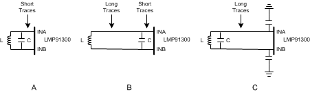 Figure 24. LC Tank Traces
8.2.2.17 SWDRV Terminal
Keep the trace between the SWDRV terminal and the transistor short.
8.2.2.18 P1 To P5 Terminals
Connect to ground using short traces.
8.2.2.19 GND Terminals
Connect to ground using short traces.
8.2.2.20 NC Terminals
These terminals do not connect to the silicon and can be left unconnected.
8.2.2.21 Exposed DAP
Connect to ground. The DAP area on the PCB can be used as the center of a star ground with all other ground terminals connecting to it.
8.2.2.22 SENSE-
In PNP mode the SENSE- terminal is not used. It should be connected to ground.
8.2.3 Look-Up Table Calibration
- RP Measurement: Take RP measurements by reading the Proximity registers 0x7A and 0x7B from the lowest temperature of interest to the highest temperature within the predefined LUT values. The temperature range should fall within the LUT preset values of -48°C to 136°C in 4°C increments. Convert all the measured values from hex to decimal.
- Proximity measurements at all temperatures between -48°C to 136°C will give the most accurate results. If the proximity measurement at some temperatures are skipped a value will need to be interpolated from the measured values. This is described in step 4.
- To avoid uncertain conditions outside the temperature range of interest the user should duplicate the same value of RP for the temperature below and above those limits. For example, if the lowest temperature that a proximity measurement was made was -28°C, this value should be used for all lower temperatures. The same applies at the high temperature range of the LUT.
- Temperature Correlation: For every RP measurement the temperature register TEMP64 (0x79) should be read to ensure that the ambient temperature correlates to the intended LUT preset temperature. The TEMP64 register is an 8 bit unsigned register that contains the temperature (in °C) + 64. Any discrepancy between ambient temperature and preset LUT temperature during calibration will result in a temperature calibration error.
- Normalizing RP: Once all RP values have been read and logged for the whole LUT temperature range as illustrated in Figure 25 the data must be normalized to the intended ambient operating temperature T0. This is done by dividing each RP data point by R0, the measured RP at the ambient operating temperature for each temperature of the LUT register. This ratio provides the gain correction factor coefficients (GCF) as shown in Figure 26. If the ambient operating temperature T0 does not fall on one of the 4°C incremental points of the LUT then R0 will need to be interpolated.
- Interpolating GCF values that have not been measured: Plot the measured GCF values vs temperature and then make a polynomial trend line of the data. Use the formula of the trend line to determine the GCF values for all temperatures that were not measured.
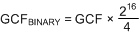
- LUT Data Entry: Each GCF needs to be converted from decimal to a 16 bit binary word representing a decimal number between 0 and 4. An example illustrating this binary representation of the decimal number is shown in Figure 27. The conversion equation that scales the GCF into the 16 bit binary GCFBINARY is shown in Equation 2. Once the conversion has been calculated for each temperature the values are programmed into the appropriate registers in the LUT. The MSB of the LUT value consists of bits D15 to D8 as shown in Figure 27, the LSB are bits D7 to D0.
- NTCs with a β ≠ 4250: The temperature LUT has been internally hard coded based on a specific NTC with a β factor of 4250 (Murata NCP03WF104F05RL). The user must recalibrate the LUT when an NTC with a β factor other than 4250 is used. The LUT temperature range is extended past the LMP91300 operating range to facilitate recalibrating the LUT if using other off the shelf NTC components. The process for using a NTC that has β ≠ 4250 is as follows:
- Put the finished system including the LC tank, NTC and LMP91300 into a temperature chamber.
- Set the temperature of the chamber to a value, for this example we will use -40°C.
- Read the temperature from register 0x79. For this example we will use -44°C.
- Follow the process above to determine the gain.
- The gain value will go into the -44°C position of the LUT.
- Connect terminals P1 - P5 to ground using short traces.
- Connect the Ground terminal to the main ground point using short traces.
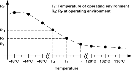 Figure 25. RP Measurement Example
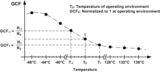 Figure 26. GCF Normalized Example
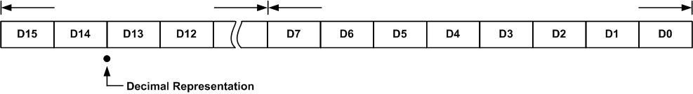 Figure 27. Binary Representation Of Gain Correction Factor