SLVS658C March 2006 – January 2016 TPS65811
PRODUCTION DATA.
- 1 Features
- 2 Applications
- 3 Description
- 4 Revision History
- 5 Description (continued)
- 6 Pin Configuration and Functions
-
7 Specifications
- 7.1 Absolute Maximum Ratings
- 7.2 ESD Ratings
- 7.3 Recommended Operating Conditions
- 7.4 Thermal Information
- 7.5 Electrical Characteristics - System Sequencing and Operating Modes
- 7.6 Electrical Characteristics - Power Path and Charge Management
- 7.7 Electrical Characteristics - Power Path and Charge Management (Continued)
- 7.8 Electrical Characteristics - Power Path and Charge Management (Continued)
- 7.9 Electrical Characteristics - Linear Regulators
- 7.10 Electrical Characteristics - Switched-Mode SM1 Step-Down Converter
- 7.11 Electrical Characteristics - Switched-Mode SM2 Step-Down Converter
- 7.12 Electrical Characteristics - GPIOs
- 7.13 Electrical Characteristics - ADC
- 7.14 Electrical Characteristics - LED and PWM Drivers
- 7.15 Electrical Characteristics - I2C Interface
- 7.16 Timing Requirements - I2C Interface
- 7.17 Trigger Timing Characteristics
- 7.18 Dissipation Ratings
- 7.19 Typical Characteristics
-
8 Detailed Description
- 8.1 Overview
- 8.2 Functional Block Diagram
- 8.3
Feature Description
- 8.3.1 Interrupt Controller and System Sequencing
- 8.3.2
Power Path and Charge Management
- 8.3.2.1 Overview
- 8.3.2.2
Power Path Management Function
- 8.3.2.2.1 Detecting the System Status
- 8.3.2.2.2 Power Path Logic: Priority Algorithm
- 8.3.2.2.3 Input Current Limit
- 8.3.2.2.4 System Voltage Regulation
- 8.3.2.2.5 Input Overvoltage Detection
- 8.3.2.2.6 Output Short-Circuit Detection
- 8.3.2.2.7 Battery Short-Circuit Detection
- 8.3.2.2.8 Initial Power Path Operation
- 8.3.2.2.9 No-Battery Detection Circuit
- 8.3.2.2.10 Using the Input Power to Run the System and Charge the Battery Pack
- 8.3.2.3
Battery Charge Management Function
- 8.3.2.3.1 Operating Modes
- 8.3.2.3.2 Battery Preconditioning
- 8.3.2.3.3 Constant Current Charging
- 8.3.2.3.4 Charge Termination and Recharge
- 8.3.2.3.5 Battery Voltage Regulation, Charge Voltage
- 8.3.2.3.6 Temperature Qualification
- 8.3.2.3.7 Dynamic Power Path Management
- 8.3.2.3.8 Charger Off Mode
- 8.3.2.3.9 Precharge Safety Timer
- 8.3.2.3.10 Charge Safety Timer
- 8.3.2.3.11 Timer Fault Recovery
- 8.3.2.3.12 Dynamic Timer Function
- 8.3.2.4 Functionality Guide — System Power and Charge Management
- 8.3.3 Linear Regulators
- 8.3.4
Step-Down Switched-Mode Converters: SM1 and SM2
- 8.3.4.1 Output Voltage Slew Rate
- 8.3.4.2 Soft-Start
- 8.3.4.3 Dropout Operation at 100% Duty Cycle
- 8.3.4.4 Output Voltage Monitoring
- 8.3.4.5 Stand-by Mode
- 8.3.4.6 PWM Operation
- 8.3.4.7 Phase Control in PWM Mode
- 8.3.4.8 PFM Mode Operation
- 8.3.4.9 Functionality Guide — Switched-Mode Step-Down Converters
- 8.3.5
Analog-to-Digital Converter
- 8.3.5.1 Overview
- 8.3.5.2 Input Channels
- 8.3.5.3
Functional Overview
- 8.3.5.3.1 ADC Conversion Cycle
- 8.3.5.3.2 External Trigger Operation
- 8.3.5.3.3 Detecting an External Trigger Event
- 8.3.5.3.4 Executing Multiple-Sample Cycles With an External Trigger
- 8.3.5.3.5 Continuous Conversion Operation (Repeat Mode)
- 8.3.5.3.6 ADC Input Signal Range Setting
- 8.3.5.3.7 ADC State Machine
- 8.3.5.4 Battery Detection Circuit
- 8.3.5.5 Functionality Guide - Analog to Digital Converter
- 8.3.6 LED and Peripheral Drivers
- 8.3.7 General-Purpose I/Os — GPIO 1, 2, 3
- 8.4 Device Functional Modes
- 8.5
Programming
- 8.5.1
Serial Interface
- 8.5.1.1 Overview
- 8.5.1.2 Register Default Values
- 8.5.1.3 I2C Address
- 8.5.1.4 Incremental Read
- 8.5.1.5 I2C Bus Release
- 8.5.1.6 Sleep Mode Operation
- 8.5.1.7 I2C Communication Protocol
- 8.5.1.8 I2C Read and Write Operations
- 8.5.1.9 Valid Write Sequences
- 8.5.1.10 One-Byte Write
- 8.5.1.11 Valid Read Sequences
- 8.5.1.12 Non-Valid Sequences
- 8.5.1
Serial Interface
- 8.6
Register Maps
- 8.6.1 Sequencing and Operating Modes - I2C Registers
- 8.6.2 System Status — I2C Registers
- 8.6.3 Interrupt Controller - I2C Registers
- 8.6.4 Charge and System Power Management — I2C Registers
- 8.6.5 Linear Regulators — I2C Registers
- 8.6.6 Switched-Mode Step-Down Converters — I2C Registers
- 8.6.7 ADC - I2C Registers
- 8.6.8 White LED, PWM Drivers — I2C Registers
- 8.6.9 GPIOs — I2C Registers
- 9 Application and Implementation
- 10Power Supply Recommendations
- 11Layout
- 12Device and Documentation Support
- 13Mechanical, Packaging, and Orderable Information
9 Application and Implementation
NOTE
Information in the following applications sections is not part of the TI component specification, and TI does not warrant its accuracy or completeness. TI’s customers are responsible for determining suitability of components for their purposes. Customers should validate and test their design implementation to confirm system functionality.
9.1 Application Information
The target application for this device is a smart phone operated from a single Lithium Ion battery that can be recharged from either a USB port or an AC adaptor.
9.2 Typical Applications
9.2.1 SM1, SM2 Converter Design Example
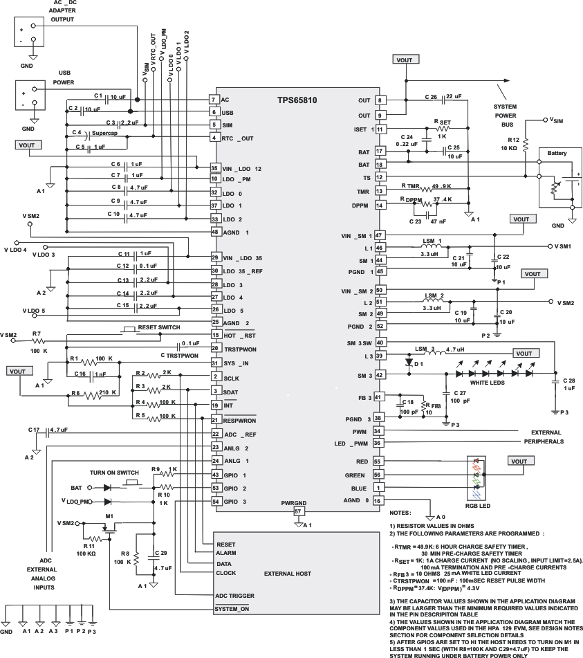 Figure 51. TPS65810 Application Diagram, Recommended External Components
9.2.1.1 Design Requirements
Use values listed in Table 45 as the design conditions and parameters for the SM1 or SM2 converter design example.
Table 45. Design Parameter
| DESIGN PARAMETER | EXAMPLE VALUE |
|---|---|
| VIN_SM1/2 | 4.6 V typical (may be less if input source is limited) |
| VOUT_SM1/2 | 1.24 V |
| IO(MAX) | 0.6 A |
| fSW | 1500 kHz |
| fC | 25 kHz |
Use Equation 13 to calculate the target inductance for this design application.

where
- 3.3 µH is a good target value
Use Equation 14 to calculate the target capacitance for this design application.

where
- 10 µ is a good target value
9.2.1.2 Detailed Design Procedure
9.2.1.2.1 Inductor and Capacitor Selection — Converters SM1 and SM2
SM1 and SM2 are designed with internal voltage mode compensation and the stabilization is based on the selection of an LC filter that has a corner frequency around 27 kHz. TI does not recommend using LC values that would be outside the range of 13 kHz to 40 kHz.
Use Equation 15 to calculate the corner frequency of the output LC filter for L = 3.3 µH and C = 10 µF which are the standard recommended LC values.

The inductor value, along with the input voltage VIN, output voltage VOUT and switching frequency f define the ripple current. Typically the ripple current target is 30% of the full load current. At light loads it is desirable for ripple current to be less then 150% of the light load current.
The inductor must be chosen with a rating to handle the peak ripple current, if a current of an inductor gets higher than its rated saturation level (DCR), the inductance starts to fall off, and the inductor’s ripple current increases exponentially. The DCR of the inductor plays an important role in efficiency and size of the inductor. Larger diameter wire has less DCR but may increase the size of the inductor
Use Equation 16 to calculate the target inductor value. If an inductor value was already selected, use Equation 17 to calculate the ripple current of the inductor under static operating conditions. The ripple amplitude can be calculated during the ON-time (positive ramp) or during the OFF-time (negative ramp). Calculating the ripple using the off time is the easiest method because the voltage of the inductor is the output voltage.


Use Equation 18 to calculate the peak current because of the output load and ripple current.

For a faster transient response, a lower inductor and higher capacitance allows the output current to ramp faster, while the addition capacitance holds up the output longer (a 2.2-μH inductor in combination with a 22-μF output capacitor are recommended).
The highest inductor current occurs at the maximum input voltage. The peak inductor current during a transient may be higher than the steady state peak current and must be considered when selecting an inductor. Monitoring the inductor current for non-saturation operation during a transient of 1.2 × ILmax at VIN_MAX ensures adequate saturation margin. Table 46 lists recommended inductors for typical operating conditions.
Table 46. Inductors for Typical Operation Conditions
| DEVICE | INDUCTOR VALUE | TYPE | COMPONENT SUPPLIER |
|---|---|---|---|
| DCDC3 converter | 3.3 μH | CDRH2D14NP-3R3 | Sumida |
| 3.3 μH | PDS3010-332 | Coilcraft | |
| 3.3 μH | VLF4012AT-3R3M1R3 | TDK | |
| 2.2 μH | VLF4012AT-2R2M1R5 | TDK | |
| 2.2 μH | NR3015T2R2 | Taoup-Uidem | |
| DCDC2 converter | 3.3 μH | CDRH2D18/HPNP-3R3 | Sumida |
| 3.3 μH | VLF4012AT-3R3M1R3 | TDK | |
| 2.2 μH | VLCF4020-2R2 | TDK | |
| DCDC1 converter | 3.3 μH | CDRH3D14/HPNP-3R2 | Sumida |
| 3.3 μH | CDRH4D28C-3R2 | Sumida | |
| 3.3 μH | MSS5131-332 | Coilcraft | |
| 2.2 μH | VLCF4020-2R2 | TDK |
9.2.1.2.2 Output Capacitor Selection, SM1, SM2 Converters
The advanced Fast Response voltage mode control scheme of the SM1, SM2 converters implemented in the TPS65020 allow the use of small ceramic capacitors with a typical value of 10 μF for a 3.3-μH inductor, without having large output voltage under and overshoots during heavy load transients.
Ceramic capacitors having low ESR values have low output voltage ripple, and recommended values and manufacturers are listed in Table 27. Often, because of the low ESR, the ripple current rating of the ceramic capacitor is adequate to meet the inductor’s currents requirements.
Use Equation 19 to calculate the RMS ripple current.

At nominal load current, the inductive converters operate in PWM mode. The overall output voltage ripple is the sum of the voltage spike caused by the output capacitor ESR plus the voltage ripple caused by charging and discharging the output capacitor: The output voltage ripple is maximum at the highest input voltage Vin. Use Equation 20 to calculate the voltage spike caused by the output capacitor ESR (VRMSCout).

At light load currents, the converters operate in PFM and the output voltage ripple is dependent on the output capacitor value. The output voltage ripple is set by the internal PFM output voltage comparator delay and the external capacitor. The typical output voltage ripple is less than 1% of the nominal output voltage. Table 47 lists recommend I/O capacitors for typical operating conditions.
Table 47. Input and Output Capacitors for Typical Operation Conditions
| CAPACITOR VALUE | CASE SIZE | COMPONENT SUPPLIER | COMMENTS |
|---|---|---|---|
| 22 μF | 1260 | TDK C3216X5R0J226M | Ceramic |
| 22 μF | 1260 | Taiyo Yuden JMK316BJ226ML | Ceramic |
| 10 μF | 0805 | Taiyo Yuden JMK212BJ106M | Ceramic |
| 10 μF | 0805 | TDK C2012X5R0J106M | Ceramic |
| 22 μF | 0805 | TDK C2012X5R0J226MT | Ceramic |
| 22 μF | 0805 | Taiyo Yuden JMK212BJ226MG | Ceramic |
9.2.1.2.3 Input Capacitor Selection, SM1, SM2 Converters
Buck converters have a pulsating input current that can generate high input voltage spikes at VIN. A low ESR input capacitor is required to filter the input voltage, minimizing the interference with other circuits connected to the same power supply rail. Each DC–DC converter requires a 10-μF ceramic input capacitor on its input pin.
9.2.1.2.4 Output Voltage Selection, SM1, SM2 Converters
Typically the output voltage is programmed by the I2C. An external divider can be added to raise the output voltage, if the available I2C values do not meet the application requirements. Take care with this special option, because this external divider (gain factor) would apply to any selected I2C output voltage value for this converter.
Use Table 46 to calculate the value of R1 with R2 = 20 kΩ.

where
- VSMxOUT is the desired output voltage and R1/R2 is the feedback divider
- VFB is the I2C selected voltage
9.2.1.3 Application Curves
The application curves were measured with the application circuit shown in Figure 51 (unless otherwise noted).
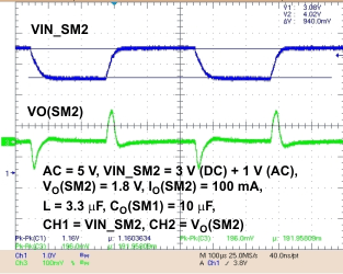 Figure 52. Line Transient
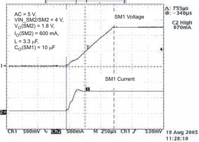 Figure 54. Transient - SM1 Start-Up
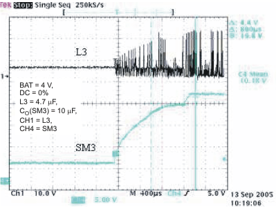 Figure 56. SM3 White LED Driver Soft-Start
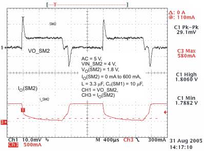 Figure 53. Load Transient
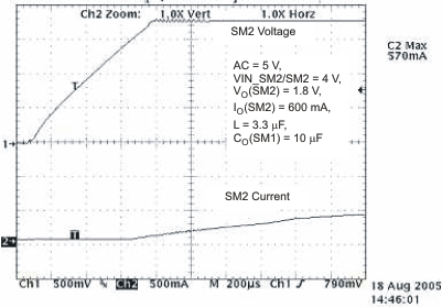 Figure 55. Transient - SM2 Start-Up
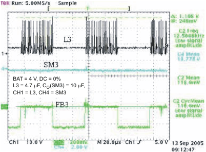 Figure 57. SM3 Led Current vs PWM Duty Cycle
9.2.2 Charger Design Example
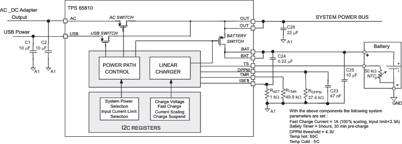 Figure 58. Required External Components, Recommended Values, External Connections
9.2.2.1 Design Requirements
Use values listed in Table 48 as the design conditions and parameters for the charger design example.
Table 48. Design Parameter
| DESIGN PARAMETER | EXAMPLE VALUE |
|---|---|
| V(OUT) | 4.6 V; (OUT pin is input to charger) |
| Fast-charge current, IPGM | 1 A |
| DPPM-OUT threshold | 4.3 V; (charging current reduces when OUT falls to this level) |
| Safety timer | 5 h |
| Battery short-circuit delay, tDELAY | 47 μs; (delays BAT short circuit during hot plug of battery) |
| TS temperature range | Disabled |
| K(SET) | 400 |
| V(SET) | 2.5 V |
| KDPPM | 1.15 |
| IDPPM | 100 μA |
| KTMR | 0.36 s/Ω |
9.2.2.2 Detailed Design Procedure
9.2.2.2.1 Program the Fast Charge Current Level:
Use Equation 22 to calculate the fast-charge current level.

9.2.2.2.2 Program the DPPM_OUT Voltage Level
Use Equation 23 to calculate the DPPM_OUT voltage level which is the level at which the charging current is reduced.

9.2.2.2.3 Program the BAT Short Circuit Delay
Use Equation 24 to calculate the BAT short-circuit delay which is used to insert the battery.

9.2.2.2.4 Program the 5-Hour Safety Timer
Use Equation 25 to calculate the value of the safety timer.
