JAJSFC7C September 2015 – July 2016 SN65DP149 , SN75DP149
PRODUCTION DATA.
- 1 特長
- 2 アプリケーション
- 3 概要
- 4 改訂履歴
- 5 概要(続き)
- 6 Pin Configuration and Functions
-
7 Specifications
- 7.1 Absolute Maximum Ratings
- 7.2 ESD Ratings
- 7.3 Recommended Operating Conditions
- 7.4 Thermal Information
- 7.5 Power Supply Electrical Characteristics
- 7.6 Differential Input Electrical Characteristics
- 7.7 HDMI and DVI TMDS Output Electrical Characteristics
- 7.8 DDC, and I2C Electrical Characteristics
- 7.9 HPD Electrical Characteristics
- 7.10 HDMI and DVI Main Link Switching Characteristics
- 7.11 HPD Switching Characteristics
- 7.12 DDC and I2C Switching Characteristics
- 7.13 Typical Characteristics
- 8 Parameter Measurement Information
- 9 Detailed Description
- 10Application and Implementation
- 11Power Supply Recommendations
- 12Layout
- 13デバイスおよびドキュメントのサポート
- 14メカニカル、パッケージ、および注文情報
パッケージ・オプション
メカニカル・データ(パッケージ|ピン)
- RSB|40
サーマルパッド・メカニカル・データ
- RSB|40
発注情報
9.3.8.1 Pre-Emphasis/De-Emphasis
The SNx5DP149 provides De-emphasis as a way to compensate for the ISI loss between the TMDS outputs and the receiver it is driving. There are two methods to implement this function. When in pin strapping mode the PRE_SEL pin controls this. The PRE_SEL pin provides –2-dB, or 0-dB de-emphasis, which allows output signal pre-conditioning to offset interconnect losses from the SNx5DP149 device outputs to a TMDS receiver. TI recommends setting PRE_SEL at 0 dB while connecting to a receiver through a short PCB route. When pulled to ground with a 65-kΩ resistor –2-dB can be realized, see Figure 9. When using I2C, Reg0Ch[1:0] is used to make these adjustments.
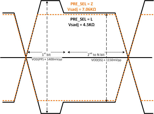
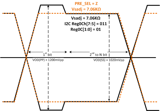
As there are times true pre-emphasis may be the best solution there are two ways to accomplish this. If pin strapping is being use the best method is to reduce the Vsadj resistor value increasing the VOD and then pulling the PRE_SEL pin to ground using the 65-kΩ resistor, see Figure 26. If using I2C this can be accomplished using two methods. First is similar to pin strapping by adjusting the Vsadj resistor value and then implementing –2-dB de-emphasis. Second method is to set Reg0Ch[7:5] = 011 and the set Reg0Ch[1:0] = 01 which accomplishes the same pre-emphasis setting. See Figure 27.
 Figure 26. Pre-Emphasis Using Pin Strapping Method
  Figure 27. Pre-Emphasis Using I2C Method