SLVS440C January 2003 – December 2014 TPS61045
PRODUCTION DATA.
- 1 Features
- 2 Applications
- 3 Description
- 4 Revision History
- 5 Pin Configuration and Functions
- 6 Specifications
- 7 Detailed Description
- 8 Application and Implementation
- 9 Power Supply Recommendations
- 10Layout
- 11Device and Documentation Support
- 12Mechanical, Packaging, and Orderable Information
パッケージ・オプション
デバイスごとのパッケージ図は、PDF版データシートをご参照ください。
メカニカル・データ(パッケージ|ピン)
- DRB|8
サーマルパッド・メカニカル・データ
- DRB|8
発注情報
5 Pin Configuration and Functions
DRB PACKAGE
(TOP VIEW)
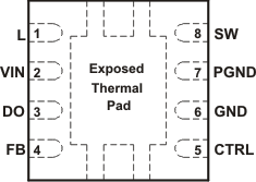
1. The exposed thermal pad is connected to PGND. Connect this pad directly with the GND pin.
Pin Functions
| PIN | I/O | DESCRIPTION | |
|---|---|---|---|
| NAME | NO. | ||
| CTRL | 5 | I | Combined enable and digital output voltage programming pin. Pulling CTRL constantly high enables the device. When CTRL is pulled to GND, the device is disabled and the input is disconnected from the output by opening the integrated switch Q1. Pulsing CTRL low increases or decreases the output voltage. Refer to Application and Implementation for further information. |
| DO | 3 | O | Internal DAC output. DO programs the output voltage through the CTRL pin. Refer to Application and Implementation for further information. |
| FB | 4 | I | Feedback. FB must be connected to the output voltage-feedback divider. |
| GND | 6 | — | Analog ground. GND must be directly connected to the PGND pin. Refer to Application and Implementation for further information. |
| L | 1 | O | Drain of the internal input switch (Q1). Connect L to the inductor. |
| PGND | 7 | — | Power ground |
| SW | 8 | I | Drain of the integrated main switch Q2. SW is connected to the inductor and anode of the Schottky rectifier diode. |
| VIN | 2 | I | Input supply pin |