SLVS658C March 2006 – January 2016 TPS65811
PRODUCTION DATA.
- 1 Features
- 2 Applications
- 3 Description
- 4 Revision History
- 5 Description (continued)
- 6 Pin Configuration and Functions
-
7 Specifications
- 7.1 Absolute Maximum Ratings
- 7.2 ESD Ratings
- 7.3 Recommended Operating Conditions
- 7.4 Thermal Information
- 7.5 Electrical Characteristics - System Sequencing and Operating Modes
- 7.6 Electrical Characteristics - Power Path and Charge Management
- 7.7 Electrical Characteristics - Power Path and Charge Management (Continued)
- 7.8 Electrical Characteristics - Power Path and Charge Management (Continued)
- 7.9 Electrical Characteristics - Linear Regulators
- 7.10 Electrical Characteristics - Switched-Mode SM1 Step-Down Converter
- 7.11 Electrical Characteristics - Switched-Mode SM2 Step-Down Converter
- 7.12 Electrical Characteristics - GPIOs
- 7.13 Electrical Characteristics - ADC
- 7.14 Electrical Characteristics - LED and PWM Drivers
- 7.15 Electrical Characteristics - I2C Interface
- 7.16 Timing Requirements - I2C Interface
- 7.17 Trigger Timing Characteristics
- 7.18 Dissipation Ratings
- 7.19 Typical Characteristics
-
8 Detailed Description
- 8.1 Overview
- 8.2 Functional Block Diagram
- 8.3
Feature Description
- 8.3.1 Interrupt Controller and System Sequencing
- 8.3.2
Power Path and Charge Management
- 8.3.2.1 Overview
- 8.3.2.2
Power Path Management Function
- 8.3.2.2.1 Detecting the System Status
- 8.3.2.2.2 Power Path Logic: Priority Algorithm
- 8.3.2.2.3 Input Current Limit
- 8.3.2.2.4 System Voltage Regulation
- 8.3.2.2.5 Input Overvoltage Detection
- 8.3.2.2.6 Output Short-Circuit Detection
- 8.3.2.2.7 Battery Short-Circuit Detection
- 8.3.2.2.8 Initial Power Path Operation
- 8.3.2.2.9 No-Battery Detection Circuit
- 8.3.2.2.10 Using the Input Power to Run the System and Charge the Battery Pack
- 8.3.2.3
Battery Charge Management Function
- 8.3.2.3.1 Operating Modes
- 8.3.2.3.2 Battery Preconditioning
- 8.3.2.3.3 Constant Current Charging
- 8.3.2.3.4 Charge Termination and Recharge
- 8.3.2.3.5 Battery Voltage Regulation, Charge Voltage
- 8.3.2.3.6 Temperature Qualification
- 8.3.2.3.7 Dynamic Power Path Management
- 8.3.2.3.8 Charger Off Mode
- 8.3.2.3.9 Precharge Safety Timer
- 8.3.2.3.10 Charge Safety Timer
- 8.3.2.3.11 Timer Fault Recovery
- 8.3.2.3.12 Dynamic Timer Function
- 8.3.2.4 Functionality Guide — System Power and Charge Management
- 8.3.3 Linear Regulators
- 8.3.4
Step-Down Switched-Mode Converters: SM1 and SM2
- 8.3.4.1 Output Voltage Slew Rate
- 8.3.4.2 Soft-Start
- 8.3.4.3 Dropout Operation at 100% Duty Cycle
- 8.3.4.4 Output Voltage Monitoring
- 8.3.4.5 Stand-by Mode
- 8.3.4.6 PWM Operation
- 8.3.4.7 Phase Control in PWM Mode
- 8.3.4.8 PFM Mode Operation
- 8.3.4.9 Functionality Guide — Switched-Mode Step-Down Converters
- 8.3.5
Analog-to-Digital Converter
- 8.3.5.1 Overview
- 8.3.5.2 Input Channels
- 8.3.5.3
Functional Overview
- 8.3.5.3.1 ADC Conversion Cycle
- 8.3.5.3.2 External Trigger Operation
- 8.3.5.3.3 Detecting an External Trigger Event
- 8.3.5.3.4 Executing Multiple-Sample Cycles With an External Trigger
- 8.3.5.3.5 Continuous Conversion Operation (Repeat Mode)
- 8.3.5.3.6 ADC Input Signal Range Setting
- 8.3.5.3.7 ADC State Machine
- 8.3.5.4 Battery Detection Circuit
- 8.3.5.5 Functionality Guide - Analog to Digital Converter
- 8.3.6 LED and Peripheral Drivers
- 8.3.7 General-Purpose I/Os — GPIO 1, 2, 3
- 8.4 Device Functional Modes
- 8.5
Programming
- 8.5.1
Serial Interface
- 8.5.1.1 Overview
- 8.5.1.2 Register Default Values
- 8.5.1.3 I2C Address
- 8.5.1.4 Incremental Read
- 8.5.1.5 I2C Bus Release
- 8.5.1.6 Sleep Mode Operation
- 8.5.1.7 I2C Communication Protocol
- 8.5.1.8 I2C Read and Write Operations
- 8.5.1.9 Valid Write Sequences
- 8.5.1.10 One-Byte Write
- 8.5.1.11 Valid Read Sequences
- 8.5.1.12 Non-Valid Sequences
- 8.5.1
Serial Interface
- 8.6
Register Maps
- 8.6.1 Sequencing and Operating Modes - I2C Registers
- 8.6.2 System Status — I2C Registers
- 8.6.3 Interrupt Controller - I2C Registers
- 8.6.4 Charge and System Power Management — I2C Registers
- 8.6.5 Linear Regulators — I2C Registers
- 8.6.6 Switched-Mode Step-Down Converters — I2C Registers
- 8.6.7 ADC - I2C Registers
- 8.6.8 White LED, PWM Drivers — I2C Registers
- 8.6.9 GPIOs — I2C Registers
- 9 Application and Implementation
- 10Power Supply Recommendations
- 11Layout
- 12Device and Documentation Support
- 13Mechanical, Packaging, and Orderable Information
7 Specifications
7.1 Absolute Maximum Ratings
over operating free-air temperature range (unless otherwise noted)(1)(1) Stresses beyond those listed under Absolute Maximum Ratings may cause permanent damage to the device. These are stress ratings only and functional operation of the device at these or any other conditions beyond those indicated under Recommended Operating Conditions is not implied. Exposure to absolute-maximum-rated conditions for extended periods may affect device reliability.
7.2 ESD Ratings
| VALUE | UNIT | |||
|---|---|---|---|---|
| V(ESD) | Electrostatic discharge | Human-body model (HBM), per ANSI/ESDA/JEDEC JS-001(1) | 1500 | V |
(1) JEDEC document JEP155 states that 500-V HBM allows safe manufacturing with a standard ESD control process.
7.3 Recommended Operating Conditions
| MIN | MAX | UNIT | |||
|---|---|---|---|---|---|
| AC and USB with respect to AGND1 | 4.35 | 16.5(1) | V | ||
| ANLG1,ANLG2 with respect to AGND2 | 0 | 2.6 | V | ||
| VIN_LDO35 with respect to AGND2 | See (2) | 4.7 | V | ||
| VIN_LDO12 with respect to AGND1 | See (2) | 4.7 | V | ||
| VIN_SM1 with respect to PGND1 | See (2) | 4.7 | V | ||
| VIN_SM2 with respect to PGND2 | See (2) | 4.7 | V | ||
| SM3 with respect to PGND3 | 28 | V | |||
| TA | Operating free-air temperature | –40 | 85 | °C | |
| TJ(op) | Junction temperature, functional operation ensured | –40 | 125 | °C | |
| TJ | Junction temperature, electrical characteristics ensured | 0 | 125 | °C | |
(1) Thermal operating restrictions are reduced or avoided if input voltage does not exceed 5 V.
(2) Greater of: 3.6 V OR minimum input voltage required for LDO/converter operation outside dropout region.
7.4 Thermal Information
| THERMAL METRIC(1) | TPS6581x | UNIT | |
|---|---|---|---|
| RTQ (QFN) | |||
| 56 PINS | |||
| RθJA | Junction-to-ambient thermal resistance | 26.9 | °C/W |
| RθJC(top) | Junction-to-case (top) thermal resistance | 10.9 | °C/W |
| RθJB | Junction-to-board thermal resistance | 4.9 | °C/W |
| ψJT | Junction-to-top characterization parameter | 0.2 | °C/W |
| ψJB | Junction-to-board characterization parameter | 4.8 | °C/W |
| RθJC(bot) | Junction-to-case (bottom) thermal resistance | 0.7 | °C/W |
(1) For more information about traditional and new thermal metrics, see the Semiconductor and IC Package Thermal Metrics application report, SPRA953.
7.5 Electrical Characteristics – System Sequencing and Operating Modes
over recommended operating conditions (typical values at TJ = 25°C), application circuit as in Figure 51 (unless otherwise noted)| PARAMETER | TEST CONDITIONS | MIN | TYP | MAX | UNIT | |
|---|---|---|---|---|---|---|
| QUIESCENT CURRENT | ||||||
| IBAT(SLEEP) | BAT pin current, sleep mode set | Input power not detected, V(BAT) = 4.2 V, Sleep mode set | 400 | μA | ||
| IBAT(DONE) | BAT pin current, charge terminated | Charger function enabled by I2C, termination detected, input power detected and selected |
3 | μA | ||
| IBAT(CHGOFF) | BAT pin current, charge function OFF | Charger function disabled by I2C, termination not detected, input power detected and selected | 3 | μA | ||
| IINP(CHGOFF) | AC or USB pin current, charge function OFF | Charger function disabled by I2C, termination not detected, input power detected and selected. All integrated supplies and drivers OFF, no load at OUT pin. | 200 | μA | ||
| UNDERVOLTAGE LOCKOUT | ||||||
| VUVLO | Internal UVLO detection threshold | NO POWER mode set at V(OUT) < VUVLO, V(OUT) decreasing | –3% | 2.5 | 3% | V |
| VUVLO_HYS | UVLO detection hysteresis | V(OUT) increasing | 120 | mV | ||
| tDGL(UVLO) | UVLO detection deglitch time | Falling voltage only | 5 | ms | ||
| SYSTEM LOW VOLTAGE THRESHOLD | ||||||
| VLOW_SYS | Minimum system voltage detection threshold | System voltage V(SYS_IN) decreasing, SLEEP mode set if V(SYS_IN) < VLOW_SYS |
0.97 | 1 | 1.03 | V |
| VHYS(LOWSYS) | Minimum system voltage detection hysteresis | V(SYS_IN) increasing | 50 | mV | ||
| tDGL(LOWSYS) | Minimum system voltage detection deglitch time | V(SYS_IN) decreasing | 5 | ms | ||
| THERMAL FAULT | ||||||
| TSHUT | Thermal shutdown | Increasing junction temperature | 165 | °C | ||
| THYS(SHUT) | Thermal shutdown hysteresis | Decreasing junction temperature | 30 | °C | ||
| INTEGRATED SUPPLY POWER FAULT DETECTION | ||||||
| VPGOOD | Power-good fault detection threshold | Falling output voltage, applies to all integrated supply outputs. Referenced to the programmed output voltage value | 84% | 90% | 96% | |
| VHYS(PGOOD) | Power-good fault detection hysteresis | Rising output voltage, applies to all integrated supply outputs. Referenced to VPGOOD threshold | 3% | 5% | 7% | |
| HOT RESET FUNCTION | ||||||
| VHRSTON | Low level input voltage | RESET mode set at V(HOT_RESET) < VHRSTON | 0.4 | V | ||
| VHRSTOFF | High level input voltage | HOT reset not active at V(HOT_RESET) > VHRSTOFF | 1.3 | V | ||
| tDGL(HOTRST) | Hot reset input deglitch | 5 | ms | |||
| SYSTEM RESET – OPEN-DRAIN OUTPUT RESPWRON | ||||||
| VRSTLO | Low level output voltage | IIL = 10 mA, V(RESPWRON ) < VRSTLO | 0 | 0.3 | V | |
| ITRSTPWON | Pullup current source | Internally connected to TRSTPWRON pin | 0.9 | 1 | 1.2 | μA |
| KRESET | Reset timer constant | TRESET = KRESET × CTRSTPWON | 1 | ms/nF | ||
7.6 Electrical Characteristics – Power Path and Charge Management
over recommended operating conditions (typical values at TJ = 25°C), circuit as in Figure 51 (unless otherwise noted)| PARAMETER | TEST CONDITIONS | MIN | TYP | MAX | UNIT | ||
|---|---|---|---|---|---|---|---|
| VOLTAGE DETECTION THRESHOLDS | |||||||
| VIN(DT) | Input Voltage detection threshold | AC detected at V(AC)– V(BAT) > VIN(DT)
USB detected at V(USB)– V(BAT) > VIN(DT) |
190 | mV | |||
| VIN(NDT) | Input Voltage removal threshold | AC not detected at V(AC)– V(BAT) < VIN(NDT)
USB not detected at V(USB)– V(BAT) < VIN(NDT) |
125 | mV | |||
| tDGL(NDT) | Power not detected deglitch | 22.5 | ms | ||||
| VSUP(DT) | Supplement detection threshold | Battery switch ON at V(BAT) – V(OUT) > VSUP(DT) | 60 | mV | |||
| VSUP(NDT) | Supplement not detected threshold | Battery switch OFF at V(BAT)– V(OUT) < VSUP(NDT) | 20 | mV | |||
| POWER PATH INTEGRATED MOSFETS CHARACTERISTICS | |||||||
| VACDO | AC switch dropout voltage | VACDO = V(AC)– V(OUT); V(AC) = 4.75 V AC input current limit set to 2.75 A (typical), IO(OUT) = 1 A |
350 | 375 | mV | ||
| VUSBDO | USB switch dropout voltage | VUSBDO = V(USB)– V(OUT); V(USB) = 4.6 V USB input current limit set to 2.75 A (typical) | I(OUT)+ I(BAT)= 0.5 A | 175 | 190 | mV | |
| I(OUT)+ I(BAT)= 0.1 A | 35 | 45 | mV | ||||
| VBATDODCH | Battery switch dropout voltage, discharge | V(BAT): 3 V → VCH(REG), I(BAT) = –1 A | 60 | 100 | mV | ||
| VBATDOCH | Battery switch dropout voltage, charge | Charger on, V(BAT): 3 V → 4.2 V, I(BAT) = 1 A | 60 | 100 | mV | ||
| POWER PATH INPUT CURRENT LIMIT | |||||||
| IINP(LIM1) | Selected input current limit, applies to USB input only | Selected input switch not in dropout, I2C settings: ISET2 = LO, PSEL = LO | 80 | 100 | mA | ||
| IINP(LIM2) | Selected Input current limit, applies to USB input only | Selected input switch not in dropout, I2C settings: ISET2 = HI, PSEL = LO | 400 | 500 | mA | ||
| IINP(LIM3) | Selected Input current limit, applies to either AC or USB input | Selected input switch not in dropout, I2C settings: ISET2 = HI OR LO, PSEL = HI |
2.75 | A | |||
| SYSTEM REGULATION VOLTAGE | |||||||
| VSYS(REG) | Output regulation voltage | VSYS(REG) = V(OUT), DPPM loop not active, selected input current limit not reached. Selected input voltage (AC or USB) > 5.1 V | 4.6 | 4.7 | V | ||
| POWER PATH PROTECTION AND RECOVERY FUNCTIONS | |||||||
| VINOUTSH | Input-to-output short-circuit detection threshold | AC and USB switches set to OFF if V(OUT) < VINOUTSH | 0.6 | V | |||
| RSH(USBSH) | OUT short circuit recovery pullup resistor | V(OUT) < 1 V, internal resistor connected from USB to OUT | 500 | Ω | |||
| RSH(ACSH) | OUT short circuit recovery pullup resistor | V(OUT) < 1 V, internal resistor connected from AC to OUT | 500 | Ω | |||
| VOVP | Overvoltage detection threshold | Rising voltage, overvoltage detected when V(AC) > VOVP or V(USB) > VOVP |
6 | 6.5 | 6.8 | V | |
| Overvoltage detection hysteresis | Falling voltage, relative to detection threshold | 0.1 | V | ||||
| VBATOUTSH | Battery-to-output short-circuit detection threshold | BAT switch set to OFF if V(BAT) – V(OUT) > VBATOUTSH | 200 | mV | |||
| KBLK(SHBAT) | Battery-to-output short-circuit blanking time constant | V(DPPM) < 1v, tBLK(SHBAT) = KBLK(SHBAT) X CDPPM, CDPPM capacitor is connected from DPPM pin to AGND1 | 1 | mS/nF | |||
| ISH(BAT) | OUT short circuit recovery pullup current source | V(BAT) – V(OUT) > VBATOUTSH, Internal current source connected between OUT and BAT | 10 | mA | |||
| RSH(BAT) | BAT short circuit recovery resistor | V(BAT)< 1 V, Internal resistor connected from OUT to BAT | 1 | kΩ | |||
| RDCH(BAT) | BAT pulldown resistor | Internal resistor connected from BAT to AGND1 when battery is not detected by ANLG1 | 500 | Ω | |||
7.7 Electrical Characteristics – Power Path and Charge Management (Continued)
over recommended operating conditions (typical values at TJ = 25°C), application circuit as in Figure 51 (unless otherwise noted)| PARAMETER | TEST CONDITIONS | MIN | TYP | MAX | UNIT | ||
| POWER PATH TIMING CHARACTERISTICS, DPPM, AND THERMAL LOOPS NOT ACTIVE, RTMR = 50 kΩ | |||||||
| tBOOT | Boot-up time | Measured from input power detection | 120 | 200 | 300 | ms | |
| tSW(ACBAT) | Switching from AC to BAT | No USB: measured from V(AC) – V(BAT) < VIN(NDT), USB detected: CE = LO (after CE hold-off time) |
50 | μs | |||
| tSW(USBBAT) | Switching from USB to BAT | No AC: measured from V(USB) – V(BAT) < VIN(NDT), USB detected: CE = LO (after CE hold-off time) |
50 | μs | |||
| tSW(PSEL) | Switching from USB to AC | Toggling I2C PSEL bit | 50 | μs | |||
| tSW(ACUSB) | Switching from AC to USB or USB to AC | AC power removed or USB power removed | 100 | μs | |||
| BATTERY REMOVAL DETECTION | |||||||
| VNOBATID | Battery ID resistor detection | ID resistor not detected at V(OUT)– V(ANLG1) < VNOBATID | 0.5 | V | |||
| tDGL(NOBAT) | Deglitch time for battery removal detection | 0.6 | 1.2 | ms | |||
| IO(ANLG1) | ANLG1 pullup current | Set through I2C bits (BATID1,BATID2) ADC_WAIT register | 00, V(OUT): 2.5 V to 4.4 V |  |
μA | ||
| 01 | 10 | ||||||
| 10 | 50 | ||||||
| 11 | 60 | ||||||
| Total accuracy | 25% | 25% | |||||
| FAST CHARGE CURRENT, V(OUT) > V(BAT) + 0.1 V, V(BAT) > VLOWV | |||||||
| IO(BAT) | Charge current range |  |
100 | 1500 | mA | ||
| V(SET) | Battery charge current set voltage | V(SET) = V(ISET1), (ISET1_1, ISET1_0) = |
11, 100% scaling | 2.475 | 2.500 | 2.525 | V |
| 10, 75% scaling | 1.875 | 1.900 | 1.925 | ||||
| 01, 50% scaling | 1.225 | 1.250 | 1.275 | ||||
| 00, 25% scaling | 0.575 | 0.600 | 0.625 | ||||
| K(SET) | Battery charge current set factor | 100 mA < IO(BAT) ≤ 1 A | 350 | 400 | 450 | ||
| 1 mA < IO(BAT) ≤ 100 mA | 100 | 400 | 1000 | ||||
| PRECHARGE CURRENT, V(OUT) > V(BAT) + 0.1 V, VBATSH < V(BAT) < VLOWV, t < t(PRECHG) | |||||||
| IO(PRECHG) | Precharge current range |  |
10 | 150 | mA | ||
| VPRECHG | Precharge set voltage | VPRECHG = V(ISET1) | 220 | 250 | 270 | mV | |
| VLOWV | Precharge to fast-charge transition | Fast charge at V(BAT) > VLOWV | 2.8 | 3 | 3.2 | V | |
| tDGL(PRE) | Deglitch time for fast charge to precharge transition | Decreasing battery voltage, RTMR = 50 kΩ | 22.5 | ms | |||
| CHARGE REGULATION VOLTAGE, V(OUT) > VO(BATREG) + 0.1 V | |||||||
| VO(BATREG) | Battery charge voltage | Voltage options, selection through I2C | 4.2 | V | |||
| 4.356 | V | ||||||
| Accuracy, TA = 25°C | –0.5% | 0.5% | |||||
| Total accuracy | –1% | 1% | |||||
| CHARGE TERMINATION, V(BAT) > VRCH, VOLTAGE REGULATION MODE SET | |||||||
| I(TERM) | Charge termination current range |  |
10 | 150 | mA | ||
| V(TERM) | Battery termination detection set voltage | V(TERM) = V(ISET1), (ISET1_1, SET1_0) = |
11, 100% scaling | 240 | 260 | 280 | mV |
| 10, 75% scaling | 145 | 160 | 175 | ||||
| 01, 50% scaling | 90 | 110 | 130 | ||||
| 00, 25% scaling | 40 | 60 | 75 | ||||
| tDGL(TERM) | Deglitch time for termination detection | V(ISET1) < V(TERM), RTMR = 50 kΩ | 22.5 | ms | |||
7.8 Electrical Characteristics – Power Path and Charge Management (Continued)
over recommended operating conditions (typical values at TJ = 25°C), circuit as in Figure 51 (unless otherwise noted)| PARAMETER | TEST CONDITIONS | MIN | TYP | MAX | UNIT | ||
|---|---|---|---|---|---|---|---|
| BATTERY RECHARGE DETECTION | |||||||
| VRCH | Recharge threshold voltage | New charge cycle starts if V(BAT) < VO(BATREG) – VRCH, after termination was detected | 80 | 100 | 130 | mV | |
| tDGL(RCH) | Deglitch time for recharge detection | RTMR = 50 kΩ | 22.5 | ms | |||
| DPPM FUNCTION | |||||||
| VDPPM | DPPM regulation point range | V(DPPM) = RDPPM × KDPPMM × IO(DPPM) | 2.6 | 4.4 | V | ||
| IO(DPPM) | DPPM pin current source | AC or USB Present | 95 | 100 | 105 | μA | |
| KDPPM | DPPM scaling factor | 1.139 | 1.15 | 1.162 | |||
| tDGL(DPPM) | DPPM de-glitch time | Status bit set indicating DPPM loop active after deglitch time, RTMR = 50 kΩ | 500 | μs | |||
| CHARGE AND PRECHARGE SAFETY TIMER | |||||||
| tCHG | Charge safety timer programmed value | Safety timer range, thermal and DPPM loop not active, tCHG = RTMR × KTMR |
3 | 5 | 10 | h | |
| KTMR | Charge timer set factor | 0.313 | 0.36 | 0.414 | s/Ω | ||
| tCHGADD | Total elapsed time when DPPM or thermal loop are active | Fast charge on, tCHGADD is the maximum add-on time added to tCHG | 2 × tCHG | h | |||
| tPRECHG | Precharge safety timer programmed value | Pre charge safety timer range, thermal and DPPM loop not active, tPRECHG = KPRE × RTMR × KTMR |
18 | 30 | 60 | min | |
| KPRE | Precharge timer set factor | 0.09 | 0.1 | 0.11 | |||
| tPCHGADD | Total elapsed time when DPPM or thermal loop are active | Precharge on, tPCHGADD is the maximum add-on time added to tPRECHG |
2 × tPRECHG | h | |||
| RTMR | External timer resistor limits | 30 | 100 | kΩ | |||
| RTMR(FLT) | Timer fault recovery pullup resistor | Internal resistor connected from OUT to BAT after safety timer timeout | 1 | kΩ | |||
| THERMAL REGULATION LOOP | |||||||
| TTHREG | Temperature regulation limit | Charge current decreased and timer extended when TJ > TTHREG | 115 | 135 | °C | ||
| CHARGER THERMAL SHUTDOWN | |||||||
| TTHCHG | Charger thermal shutdown | Charger turned off when TJ > TTHCHG | 150 | °C | |||
| THCHGHYS | Charger thermal shutdown hystersis | 30 | °C | ||||
7.9 Electrical Characteristics – Linear Regulators
over recommended operating conditions (typical values at TJ = 25°C), application circuit Figure 51 (unless otherwise noted)| PARAMETER | TEST CONDITIONS | MIN | TYP | MAX | UNIT | ||
|---|---|---|---|---|---|---|---|
| SELECTABLE OUTPUT VOLTAGE LDOs: LDO1, LDO2 | |||||||
| IQ(LDO12) | Quiescent current, either LDO1 or LDO2 enabled, LDO0 disabled | IQ(LDO12) = I(VIN_LDO02) | I(LDO1,2) = –1 mA | 15 | μA | ||
| I(LDO1,2) = –150 mA | 160 | ||||||
| IO(LDO1,2) | Output current range | 150 | mA | ||||
| VO(LDO1,2) | LDO1, LDO2 Output Voltage | Output voltage, selectable through I2C. | Available output voltages: VO(LDO1,2)TYP = 1.25, 1.5, 1.8, 2.5, 2.85, 3, 3.2, 3.3 | V | |||
| Dropout voltage, 150-mA load | 300 | mV | |||||
| Total accuracy, V(VIN_LDO02) = 3.65 V | –3% | 3% | |||||
| Line Regulation, 100-mA load, V(VIN_LDO02): V(LDO1,2)TYP + 0.5 V → 4.7 V |
–1% | 1% | |||||
| Load regulation, load: 10 mA → 150 mA V(VIN_LDO02) > VO(LDO1,2) TYP + 0.5 V |
–1.5% | 1.5% | |||||
| PSR(LDO12) | PSRR at 20 kHz | 150mA load at output, V(VIN_LDO02) – VO(LDO1,2) = 1 V | 40 | dB | |||
| ISC(LDO1,2) | LDO1&2 short circuit current limit | Output grounded | 300 | mA | |||
| RDCH(LDO1,2) | Discharge resistor | LDO disabled by I2C command | 300 | Ω | |||
| ILKG(LDO1,2) | Leakage current | LDO off | 2 | μA | |||
| SIM LINEAR REGULATOR | |||||||
| IQ(SIM) | Quiescent current | Internally connected to OUT pin | 20 | μA | |||
| IO(SIM) | Output current range | 8 | mA | ||||
| VO(SIM) | SIM LDO output voltage | Output voltage, selectable through I2C. | Available output voltages: VO(SIM)TYP = 1.8 or 2.5 |
V | |||
| Dropout voltage, 8-mA load | 0.2 | V | |||||
| Total accuracy, V(OUT): 3.2 V to 4.7 V, 8 mA | –5% | 5% | |||||
| Load regulation, load: 1 mA → 8 mA, V(OUT) > VO(SIM) TYP + 0.5 V | –3% | 3% | |||||
| Line regulation, 5-mA load, V(OUT): VO(SIM) TYP + 0.5 V → 4.7 V | –2% | 2% | |||||
| ISC(SIM) | Short-circuit current limit | Output grounded | 20 | mA | |||
| ILKG(SIM) | Leakage current | LDO off | 1 | μA | |||
| PROGRAMMABLE OUTPUT VOLTAGE LDOs: LDO3, LDO4, LDO5 | |||||||
| IQ(LDO35) | Quiescent current, only one of LDO3, LDO4, LDO5 is enabled | IQ(LDO35) = I(VIN_LDO35) | 70 | μA | |||
| IO(LDO35) | Output current range | 100 | mA | ||||
| VO(LDO35) | LDO3, LDO4, LDO5 output voltage | Output voltage, selectable through I2C |
Available output voltages: VO(LDO35)TYP = 1.224 V to 4.46 V, 25-mV steps |
V | |||
| Dropout voltage, 100-mA load | 240 | mV | |||||
| Total accuracy, 100-mA load V(VIN_LDO35) = 5 V | –3% | 3% | |||||
| Load regulation, V(VIN_LDO35) > VO(LDO35)TYP + 0.5 V, load: 1 mA → 50 mA |
–1% | 1% | |||||
| Line regulation, 10-mA load, V(VIN_LDO35): VO(LDO35)TYP + 0.5 V → 4.7 V |
–1% | 1% | |||||
| ISC(LDO35) | Short-circuit current limit | Output grounded | 250 | mA | |||
| PSR(LDO35) | PSRR at 10 kHz | V(VIN_LDO35) > VO(LDO3,5) + 1 V, 50-mA load at output | 40 | dB | |||
| RDCH(LDO35) | Discharge resistor | LDO is disabled by I2C command | 400 | Ω | |||
| ILKG(LDO35) | Leakage current | LDO off | 1 | μA | |||
| RTC_OUT LINEAR REGULATOR | |||||||
| IQ(RTC_OUT) | Quiescent current for RTC LDO | Internally connected to OUT pin | 20 | μA | |||
| IO(RTC_OUT) | Output current range | 8 | mA | ||||
| VO(RTC_OUT) | RTC_OUT output voltage | Fixed output voltage value | 1.5 | V | |||
| Dropout voltage, I(RTC_OUT) = –8 mA | 200 | mV | |||||
| Total accuracy, V(OUT): 2 V to 4.7 V, 8-mA load, sleep mode not set | –5% | 5% | |||||
| Load regulation, load: 1 mA → 8 mA, 2 V < V(OUT) < 4.7 V |
–3% | 3% | |||||
| Line regulation, 5-mA load, V(OUT): 2 V → 4.7 V | –2% | 2% | |||||
| ISH(RTC_OUT) | Short-circuit current limit | V(RTC_OUT) = 0 V | 20 | mA | |||
| ILKG(RTC_OUT) | Leakage current | V(RTC_OUT) = 1.5 V, V(OUT) = 0 V | TJ = 85°C | 880 | nA | ||
| TJ = 25°C | 250 | ||||||
| LDO0 LINEAR REGULATOR | |||||||
| IQ(LDO0) | Quiescent current | Internally connected to VIN_LDO12 pin |
I(LDO0) = –1 mA | 15 | μA | ||
| I(LDO0) = –150 mA | 160 | ||||||
| IO(LDO0) | Output current range | 150 | mA | ||||
| VO(LDO0) | Output voltage | Fixed output voltage value | 3.3 | V | |||
| Dropout voltage, I(LDO0) = –150 mA | 300 | mV | |||||
| Total accuracy | –3% | 3% | |||||
| Line regulation, V(OUT): VO(LDO0) + 0.5 → 4.7 V, I(LDO0) = –100 mA |
–1% | 1% | |||||
| Load regulation, I(LDO0) = –10 mA → –150 mA | –1.5% | 1.5% | |||||
| PSR(LDO0) | PSRR at 20 kHz | 150-mA load at output, V(VIN_LDO12) – VO(LDO1,2) = 1 V | 40 | dB | |||
| ISC(LDO0) | Short circuit current limit | V(LDO0) = 0 V | 300 | mA | |||
| ILKG(LDO0) | Leakage current | LDO off | 1 | μA | |||
| LDO_PM LINEAR REGULATOR | |||||||
| IQ(LD0_PM) | Output current range | 20 | mA | ||||
| VO(LDO_PM) | Output voltage | Fixed output voltage value, V(OUT) > 4 V | 3.3 | V | |||
| Dropout voltage, I(LDOPM) = –12 mA | 0.5 | 0.7 | |||||
| Total accuracy | –5% | 5% | |||||
| ILKG(LDOPM) | Leakage current | LDO off | 1 | μA | |||
7.10 Electrical Characteristics – Switched-Mode SM1 Step-Down Converter
over recommended operating conditions (typical values at TJ = 25°C), VO(SM1) = 1.24 V, application circuit Figure 51 (unless otherwise noted)| PARAMETER | TEST CONDITIONS | MIN | TYP | MAX | UNIT | ||
|---|---|---|---|---|---|---|---|
| IQ(SM1) | Quiescent current for SM1 | IQ(SM1) = I(VIN_ SM1), no output load, not switching | 10 | μA | |||
| SM1 OFF, set through I2C | 0.1 | ||||||
| IO(SM1) | Output current range | Vin = 4.2 V, Vout = 1.24 V (TPS65810) | 600 | mA | |||
| Vin = 4.2 V, Vout = 1.24 V (TPS65811) | 750 | ||||||
| VO(SM1) | Output voltage, PWM mode | Output voltage, selectable through I2C, Standby OFF | Available output voltages: VO(SM1)TYP = 0.6 V to 1.8 V, adjustable in 40-mV steps | V | |||
| VO(SM1) = VSBY(SM1), Output voltage range, Standby ON | Available output voltages: VSBY(SM1) = 0.6 V to 1.8 V, adjustable in 40-mV steps | ||||||
| Total accuracy, VO(SM1)TYP = VSBY(SM1) = 1.24 V, V(VIN_SM1) = 3.0 V to 4.7 V; 0 mA ≤ IO(SM1) ≤ 600 mA |
–3% | 3% | |||||
| Line Regulation, V(VIN_SM1): 3.0 → 4.70 V, IO(SM1) = 10 mA |
0.027 | %/V | |||||
| Load Regulation, V(VIN_SM1) = 4.7 V, IO(SM1): 60 mA → 540 mA |
0.139 | %/A | |||||
| RDSON(PSM1) | P-channel MOSFET ON-resistance | V(VIN_SM1) = 3.6 V, 100% duty cycle set | 310 | 500 | mΩ | ||
| ILKG(PSM1) | P-channel leakage current | 0.1 | μA | ||||
| RDSON(NSM1) | N-channel MOSFET ON-resistance | V(VIN_SM1) = 3.6 V, 0% duty cycle set | 220 | 330 | mΩ | ||
| ILKG(PSM1) | N-channel leakage current | 5 | μA | ||||
| ILIM(SM1) | P- and N-channel current limit | 3 V < V(VIN_SM1) < 4.7 V (TPS65810) | 900 | 1050 | 1200 | mA | |
| 3 V < V(VIN_SM1) < 4.7 V (TPS65811) | 1000 | 1200 | 1400 | ||||
| fS(SM1) | Oscillator frequency | PWM mode set | 1.3 | 1.5 | 1.7 | MHz | |
| EFF(SM1) | Efficiency | V(VIN_SM1) = 4.2 V, PWM mode, IO(SM1) = 300 mA, VO(SM1) = 3 V |
90% | ||||
| tSS(SM1) | Soft-start ramp time | Converter OFF→ON, VO(SM1): 5% → 95% of target value | 750 | μs | |||
| tDLY(SM1) | Converter turnon delay | GPIO1 pin programmed as SM1 converter enable control. Measured from V(GPIO1): LO → HI | 170 | μs | |||
7.11 Electrical Characteristics – Switched-Mode SM2 Step-Down Converter
over recommended operating conditions (typical values at TJ = 25°C), VO(SM1) = 1.24 V, application circuit Figure 51 (unless otherwise noted)| PARAMETER | TEST CONDITIONS | MIN | TYP | MAX | UNIT | ||
|---|---|---|---|---|---|---|---|
| IQ(SM2) | Quiescent current for SM2 | IQ(SM2) = I(VIN_ SM2), no output load, not switching | 10 | μA | |||
| SM2 OFF, set through I2C | 0.1 | ||||||
| IO(SM2) | Output current range | Vin = 4.2 V, Vout = 1.24 V (TPS65810) | 600 | mA | |||
| Vin = 4.2 V, Vout = 1.24 V (TPS65811) | 750 | ||||||
| VO(SM2) | Output voltage | Output voltage, selectable through I2C, stand-by OFF | Available output voltages: VO(SM2)TYP = 1 V to 3.4 V, adjustable in 80-mV steps | V | |||
| VO(SM2) = VSBY(SM2), Output voltage range, stand-by ON | Available output voltages: VSBY(SM2) = 1 V to 3.4 V, adjustable in 80-mV steps | ||||||
| Total accuracy, VO(SM2)TYP = VSM2(SBY) = 1.8 V, V(VIN_SM2) = greater of [3.0 V or (VO(SM2) + 0.3 V)] to 4.7 V; 0 mA ≤ IO(SM2) ≤ 600 mA |
–3% | 3% | |||||
| Line regulation, V(VIN_SM2) = greater of [3 V or (VO(SM2) + 0.3 V)] to 4.7 V; 0 mA ≤ IO(SM2) ≤ 600 mA |
0.027 | %/V | |||||
| Load regulation, V(VIN_SM2) = 4.7 V, IO(SM2): 60 mA → 540 mA |
0.139 | %/A | |||||
| RDSON(PSM2) | P-channel MOSFET ON-resistance | V(VIN_SM2) = 3.6 V, 100% duty cycle set | 310 | 500 | mΩ | ||
| ILKG(PSM2) | P-channel leakage current | 0.1 | μA | ||||
| RDSON(NSM2) | N-channel MOSFET ON-resistance | V(VIN_SM2) = 3.6 V, 0% duty cycle set | 220 | 330 | mΩ | ||
| ILKG(PSM2) | N-channel leakage current | 5 | μA | ||||
| ILIM(SM2) | P- and N-channel current limit | 3 V < V(VIN_SM2) < 4.7 V (TPS65810) | 900 | 1050 | 1200 | mA | |
| 3 V < V(VIN_SM2) < 4.7 V (TPS65811) | 1000 | 1200 | 1400 | ||||
| fS(SM2) | Oscillator frequency | PWM mode set | 1.3 | 1.5 | 1.7 | MHz | |
| EFF(SM2) | Efficiency | V(VIN_SM2) = 4.2 V, IO(SM2) = 300 mA, VO(SM2) = 3 V |
90% | ||||
| tSS(SM2) | Soft-start ramp time | Converter OFF→ON, VO(SM2) : 5% → 95% of target value | 750 | μs | |||
| tDLY(SM2) | Converter turnon delay | GPIO2 pin programmed as SM2 converter enable control. Measured from V(GPIO2): LO → HI | 170 | μs | |||
7.12 Electrical Characteristics – GPIOs
over recommended operating conditions (typical values at TJ = 25°C), application circuit as in Figure 51 (unless otherwise noted).| PARAMETER | TEST CONDITIONS | MIN | TYP | MAX | UNIT | |
|---|---|---|---|---|---|---|
| GPIO1–3 | ||||||
| VOL | Low level output voltage GPIO0 | IOL = 20 mA | 0.5 | V | ||
| IOGPIO | Low level sink current into GPIO1,2,3 | V(GPIOn) = V(OUT) | 20 | mA | ||
| VIL | Low level input voltage | 0.4 | V | |||
| ILKG(GPIO) | Input leakage current | V(GPIOn) = V(OUT) | 1 | μA | ||
7.13 Electrical Characteristics – ADC
over recommended operating conditions (typical values at TJ = 25°C), V(ADC_REF) =2.535 V if external reference voltage is used, application circuit as in Figure 51 (unless otherwise noted)| PARAMETER | TEST CONDITIONS | MIN | TYP | MAX | UNIT | ||
|---|---|---|---|---|---|---|---|
| ANALOG INPUTS | |||||||
| VRNG(CH1_5) | Full scale input range Ch1 to Ch5 | Positive inputs (active clamp) Full scale ~ 2.535 V |
0 | V(ADC_REF) | V | ||
| VRNG(CH6_8) | Full scale input range Ch6 to Ch8 | Positive inputs (active clamp), full scale ~4.7 V | 0 | VINTREF ×1.854 | V | ||
| CIN(ADC) | Input capacitance (all channels) | 15 | pF | ||||
| RINADC(CH1_5) | Input resistance | (Ch1 to Ch5) | 1 | MΩ | |||
| ILKGADC(CH1_5) | Leakage current | (Ch1 to Ch5) | 100 | nA | |||
| RINADC(CH6_8) | Input resistance | (Ch6 to Ch8) | 430 | 540 | kΩ | ||
| ILKGADC(CH6_8) | Leakage current | (Ch6 to Ch8) | 10 | μA | |||
| VCH5(ADC) | Internal voltage proportional to junction temperature | TJ = 25°C, ADC channel 5 input voltage | 1.895 | V | |||
| Temperature coefficient | 6.5 | mV/ °C | |||||
| DC ACCURACY | |||||||
| RES(ADC) | Resolution | SAR ADC | 10 | Bits | |||
| MCD(ADC) | No missing codes | SPECIFIED | |||||
| INL(ADC) | Integral linearity error | ±3 | LSB | ||||
| DNL(ADC) | Differential non-linearity error | ±1 | LSB | ||||
| OFFZERO(ADC) | Offset error | Difference between the first code transition (00...00 to 00...01) and the ideal AGND + 1 LSB | 5 | LSB | |||
| OFFCH(ADC) | Offset error match between channels | 5 | LSB | ||||
| GAINADC | Gain error | Deviation in code from the ideal full scale code (11…111) for the full scale voltage | ±8 | LSB | |||
| GAINCH(ADC) | Gain error match | Any two channels | 2 | LSB | |||
| THROUGHPUT SPEED | |||||||
| ADCCLK | Sampling clock | 600 | 750 | 900 | kHz | ||
| ADCTCONV | Conversion time | Sampling, conversion and setting Rs ≤ 200 K for CH1,CH2,CH3; Rs ≤ 500 Ω for CH6, CH7, CH8 | 44 | 59 | 68 | μs | |
| REFERENCE VOLTAGES | |||||||
| VINTREF | Internal ADC reference voltage | TA = 25°C, V(ADC_REF)=VINTREF when internal ADC reference is selected | 2.53 | 2.535 | 2.54 | V | |
| ISHRT(INTREF) | Internal reference short circuit limit | V(ADC_REF)= AGND1, internal reference enabled through I2C | 6 | mA | |||
| VREF(DRIFT) | ADC internal reference temperature drift | 50 | 100 | ppm/°C | |||
| IQ(ADC) | ADC Internal reference quiescent current | Measured at OUT pin (internal reference) or ADC_REF pin (external reference) | 40 | μA | |||
| I(ANLG2) | ANLG2 pin internal pullup current source | ADC channel 2 bias current, set through I2C register ADC_WAIT bits (ADC_CH2I_D1_1, ADC_CH2I _D2) | 00 | 0 | μA | ||
| 01 | 10 | ||||||
| 10 | 50 | ||||||
| 11 | 60 | ||||||
| Total accuracy, relative to selected value | –25% | 25% | |||||
| I(ANLG1) | ANLG1 pin internal pullup current source | ADC channel 1 bias current, set through I2C register ADC_WAIT bits (BATIDI_D1, BATIDI _D2) | 00 |  |
μA | ||
| 01 | 10 | ||||||
| 10 | 50 | ||||||
| 11 | 60 | ||||||
| Total accuracy | 10% | 10% | |||||
| INTERNAL REFERENCE POWER CONSUMPTION | |||||||
| PDACTIVE | Power dissipation | Conversion active | 2.3 | mW | |||
| PDARMED | Power dissipation | Not converting | 0.43 | mW | |||
7.14 Electrical Characteristics – LED and PWM Drivers
over recommended operating conditions (typical values at TJ = 25°C), application circuit as in Figure 51 (unless otherwise noted)| PARAMETER | TEST CONDITIONS | MIN | TYP | MAX | UNIT | ||
|---|---|---|---|---|---|---|---|
| SM3 BOOST CONVERTER, WHITE LED CONSTANT CURRENT DRIVER | |||||||
| VVIN(SM3) | Input voltage range | V(OUT) = 3.3 V | 3 | 4.7 | V | ||
| VOVP3 | Output overvoltage trip | OVP detected at V(SM3) > VOVP3 | 26.5 | 29 | 30 | V | |
| VHYS(OVP3) | Output overvoltage hysteresis | OVP not detected at V(SM3) < VOVP3 – VHYS(OVP3) | 1.8 | V | |||
| VSM3REF | LED current-sense threshold | LED current below regulation point at V(FB3) < VSM3REF |
244 | 252 | 260 | mV | |
| IO(SM3) | LED current | Current range, Vin = 3.3 V,  |
0 | 25 | mA | ||
| Total accuracy, IO(SM3) = 10 mA | –10% | 10% | |||||
| DSM3SW | LED-switch duty cycle | Duty cycle range | DSM3SW = 0% to 99.6%, set through I2C, 256 steps, 0.4% minimum step |
||||
| FREP_SM3 | LED-switch duty cycle pattern repetition rate | 256 pulses within repetition rate time | SM3_LF_OSC = 0 | 122 | Hz | ||
| SM3_LF_OSC = 1 | 183 | ||||||
| RDSON(SM3SW) | LED switch MOSFET ON-resistance | V(OUT) = 3.6 V; I(SM3SW) = 20 mA | 1 | 2 | Ω | ||
| ILKG(SM3SW) | LED switch MOSFET leakage | 1 | μA | ||||
| RDSON(L3) | Power stage MOSFET ON-resistance | V(OUT) = 3.6 V; I(L3) = 200 mA | 300 | 600 | mΩ | ||
| ILKG(L3) | Power stage MOSFET leakage | 1 | μA | ||||
| IMAX(L3) | Power stage MOSFET current limit | 3 V < V(OUT) < 4.7 V | 400 | 500 | 600 | mA | |
| PWM DRIVER, PWM OPEN-DRAIN OUTPUT | |||||||
| VOL(PWM) | Low level output voltage | I(PWM) = 150 mA | 0.5 | V | |||
| FPWM | PWM driver frequency | Frequency range | Set through I2C, FPWM = 0.5 / 1 / 1.5 / 2 / 3 / 4.5 / 7.8 / 15.6 | Hz | |||
| Total accuracy, relative to selected value | –20% | 20% | |||||
| DPWM | PWM driver duty cycle | Duty cycle range | DPWM = 6.25% to 100%, set through I2C, 6.25% minimum step |
||||
| LED_PWM DRIVER, LED_PWM OPEN-DRAIN OUTPUT | |||||||
| DLEDPWM | LED_PWM driver duty cycle | Duty cycle range | DLEDPWM = 0% to 99.6%, set through I2C, 256 steps 0.4% minimum step |
||||
| FREP(LEDPWM) | LED_PWM driver duty cycle pattern repetition rate | 256 pulses within repetition rate time | SM3_LF_OSC = 0 | 122 | Hz | ||
| SM3_LF_OSC = 1 | 180 | ||||||
| VOL(LEDPWM) | Low level output voltage | I(LED_PWM) = 150 mA | 0.5 | V | |||
| VOH(LEDPWM) | High level output voltage | 6 | V | ||||
| RGB DRIVER, RED, GREEN, AND BLUE OPEN-DRAIN OUTPUT | |||||||
| tFLASH(RGB) | Flashing period | Flashing period range | tFLASH(RGB) = 1 to 8 sec, set through I2C, 0.5 s minimum step, 8 steps | s | |||
| Total accuracy | –20% | 20% | |||||
| tFLASH(ON) | Flash on time | Flash on time range, value selectable by I2C | Set through I2C, tFLASH(ON) = 0.1 / 0.15 / 0.2 / 0.25 / 0.3 / 0.4 / 0.5 / 0.6 | s | |||
| Total accuracy relative to selected value | –20% | 20% | |||||
| DRGB | Duty cycle | Duty cycle range, value selectable through I2C | DRGB = 0% to 99.98%, set through I2C, 3.23% minimum step | ||||
| ISINK(RGB) | RGB output sink current | V(RED) = V(GREEN) = V(BLUE) = 2 V, set through I2C RGB_ISET1,0 | 00 = (Driver set to OFF) | mA | |||
| 01 | 2.4 | 4 | 5.6 | ||||
| 10 | 4.8 | 8 | 11.2 | ||||
| 11 | 7 | 12 | 16.6 | ||||
| VOL(RGB) | Low-level output voltage | Output low voltage, 8-mA load, RED/GREEN/BLUE PINS | 0.3 | V | |||
| ILKG(RGB) | Output off leakage current | V(RED) = V(GREEN) = V(BLUE) = 4.7 V, all drivers disabled | 1 | μA | |||
7.15 Electrical Characteristics – I2C Interface
over recommended operating conditions (typical values at TJ = 25°C), application circuit as in Figure 51 (unless otherwise noted)| PARAMETER | TEST CONDITIONS | MIN | TYP | MAX | UNIT | |
|---|---|---|---|---|---|---|
| I2C INTERFACE LOGIC LEVELS | ||||||
| VIH | High level input voltage | 1.3 | 6 | V | ||
| VIL | Low level input voltage | 0 | 0.6 | V | ||
| IH | Input bias current | 0.01 | μA | |||
7.16 Timing Requirements – I2C Interface
over recommended operating conditions (typical values at TJ = 25°C), application circuit as in Figure 51 (unless otherwise noted)| MIN | MAX | UNIT | ||
|---|---|---|---|---|
| I2C TIMING CHARACTERISTICS | ||||
| tR | SCLK/SDATA rise time | 300 | ns | |
| tF | SCLK/SDATA fall time | 300 | ns | |
| tW(H) | SCLK pulse width, high | 600 | ns | |
| tW(L) | SCLK pulse width, low | 1.3 | μs | |
| tSU(STA) | Setup time for START condition | 600 | ns | |
| tH(STA) | START condition hold time after which first clock pulse is generated | 600 | ns | |
| tSU(DAT) | Data setup time | 100 | ns | |
| tH(DAT) | Data hold time | 0 | ns | |
| tSU(STOP) | Setup time for STOP condition | 600 | ns | |
| t(BUF) | Bus free time between START and STOP condition | 1.3 | μs | |
| FSCL | Clock Frequency | 400 | kHz | |
7.17 Trigger Timing Characteristics
| MIN | NOM | MAX | UNIT | |||
|---|---|---|---|---|---|---|
| tDELAY(TRG) | Trigger delay time accuracy | Time range, set through I2C register ADC_DELAY | 0 | 750 | µs | |
| Relative to typical value set through I2C | –20% | 20% | ||||
| tWAIT(TRG) | Trigger wait time accuracy | Time range, set through I2C register ADC_WAIT | 0 | 20.48 | ms | |
| Relative to typical value set through I2C | –20% | 20% | ||||
7.18 Dissipation Ratings
| PACKAGE | θJA | TA ≤ 55°C POWER RATING |
DERATING FACTOR ABOVE TA = 55°C |
|---|---|---|---|
| RTQ (1) (2) | 21.7°C/W | 3.22 W | 0.046 W/°C |
(1) This data is based on using the JEDEC High-K board and the exposed die pad is connected to a Cu pad on the board. This is connected to the ground plane by a via matrix.
(2) The RTQ package MSL level: HIR3 at 260°C
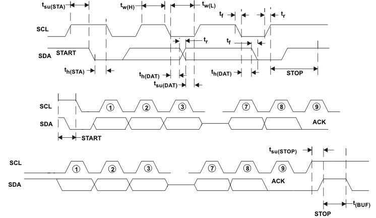 Figure 1. I2C Timing
7.19 Typical Characteristics
7.19.1 Power Path Management
These curves were measured with application circuit shown in Figure 51 (unless otherwise noted).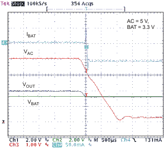 Figure 2. Switching From AC to Battery on AC Removal
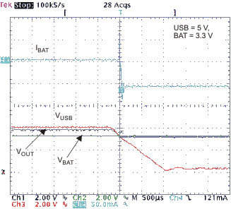 Figure 3. Switching From USB to Battery on USB Removal
7.19.2 Linear Regulators 0, 1, 2
These curves were measured with the application circuit shown in Figure 51 (unless otherwise noted).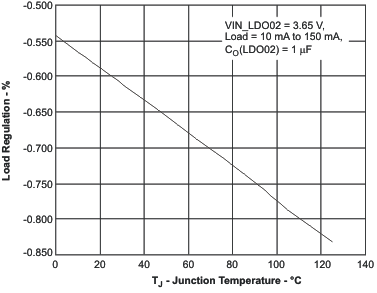 Figure 4. Load Regulation vs Junction Temperature
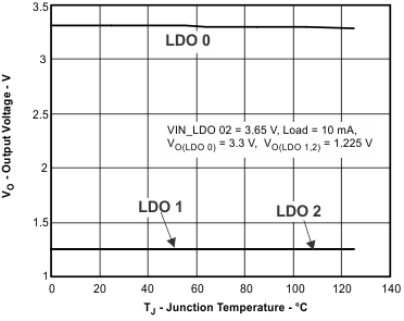 Figure 6. Output Voltage vs Junction Temperature
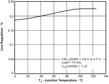 Figure 5. Line Regulation vs Junction Temperature
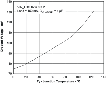 Figure 7. Dropout Voltage vs Junction Temperature
7.19.3 Linear Regulators 3, 4, 5
These curves were measured with the application circuit shown in Figure 51 (unless otherwise noted).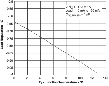 Figure 8. Load Regulation vs Junction Temperature
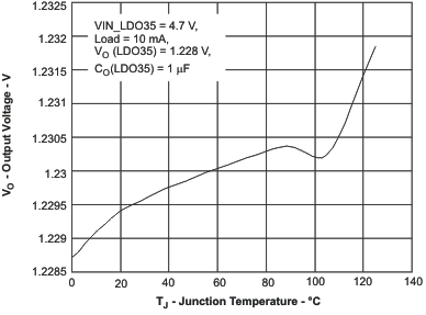 Figure 10. Output Voltage vs Junction Temperature
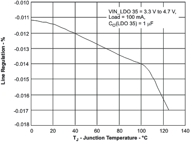 Figure 9. Line Regulation vs Junction Temperature
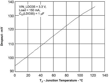 Figure 11. Dropout Voltage vs Junction Temperature
7.19.4 SM1 and SM2 Buck Converters
These curves were measured with the application circuit shown in Figure 51 (unless otherwise noted).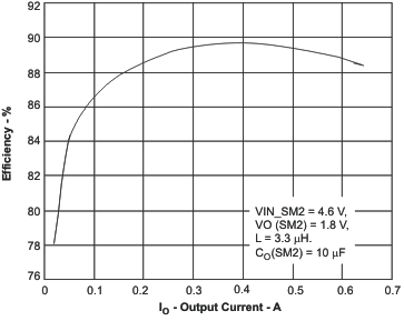 Figure 12. Efficiency in Automatic PWM/PFM Mode
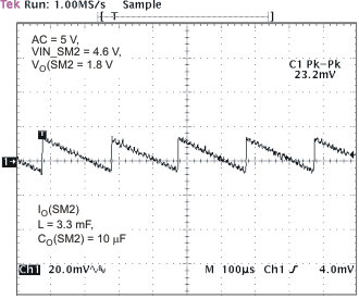 Figure 14. PFM Operation
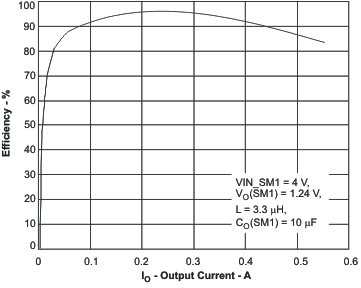 Figure 13. PWM Mode Efficiency vs Output Current
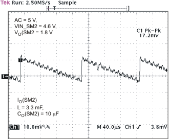 Figure 15. PFM Low Ripple Operation